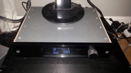
My larger 2.42" display turned up today from Hong Kong so I was all excited.
Is it SSD1306 OLED? Can you post the link here? I have hard time finding SSD1306 2.42" OLEDs on ebay.
Yep, this is the link but it does not look like he has any other items for sale at the moment 🙁. So looks like I got lucky.
Thanks, that's the exact same one I bought. For some reason, it does not show up in search results on belgian ebay, not even by item number. But it seems there are more than 10 available still.
Here's another one that does not show up in search results, but not sure what that is. There is a lot of controversial information for it:
2.42" White 128x64 OLED SSD1306 / 1309 Display for or Arduino, PIC, SPI, I2C | eBay
2.42" White 128x64 OLED SSD1306 / 1309 Display for or Arduino, PIC, SPI, I2C | eBay
Is the SSH1106 compatible ?
I found this on Ebay:
"About control chip SSH1106: SSG1106 compatible with SSD1306 basic, difference is that SSH1106 control chip RAM space is 132*64, while SSD1306 space is 128*64.
The 1.3-inch OLED 128*64 dot matrix, so in the middle of the screen production took 128 row. When using SSD1306 program point SSH1106 screen, only need to change address to 0x02 row to start."
Is it true ?
Is the SSH1106 compatible ?
I found this on Ebay:
"About control chip SSH1106: SSG1106 compatible with SSD1306 basic, difference is that SSH1106 control chip RAM space is 132*64, while SSD1306 space is 128*64.
The 1.3-inch OLED 128*64 dot matrix, so in the middle of the screen production took 128 row. When using SSD1306 program point SSH1106 screen, only need to change address to 0x02 row to start."
Is it true ?
Looks like it's not that simple:
Cheap/Small OLED Displays - SSD1306 vs SH1106 Driver | AVR Freaks
Is it SSD1306 OLED? Can you post the link here? I have hard time finding SSD1306 2.42" OLEDs on ebay.
It seems like this guy, where I bought mine, still have some??:
Great deals from BitStudio Dev | eBay Stores
Turned out mine was blue , when it arrived, but that was ok for me.
My only problem was the vertical streak...Probably just a bad sample.
By the way, the volume control sounds fantastic, by a wide margin the best I have tried...
Attachments
Yes, if you search on ebay.com, you easily get a lot more hits for these OLEDs, even though they ship worldwide.
Well I took the drastic action of cutting the PCB trace between RSH BIAS line and D7 on the Nano to allow me access to the circuit. With the line open there is a huge drop in volume as the FET gets driven but no bump.
I'm definatly getting out of my depth now but could it be overshoot in the PWM filter? If place an 10uf cap between the gate and ground the bump gets larger still. Maybe there needs to be a more gradual change to the value during cross over?
Found a bit of noise on the BIAS line to the trim pots, not that I think that has anything to do with it. Most of it was cleared down by putting a 0.1uf cap over the line to ground.
I'm definatly getting out of my depth now but could it be overshoot in the PWM filter? If place an 10uf cap between the gate and ground the bump gets larger still. Maybe there needs to be a more gradual change to the value during cross over?
Time to enjoy some music instead? (more of a note to myself 😉
Signal drop at the gate (R31) must happen at the same time with the same slope shape as voltage drop at R34 to maintain constant Id at crossover point. This is not happening. Put a scope channel 1 at the gate and channel 2 at D7; set trigger to up/down with ch1 as source and time scale at 10ms. Turn the encoder and watch the edges. The difference between two slopes will result in Vgs and Id fluctuation.
PWM pin (D3) loads a RC network, D7 has nothing on it's way to a perfect edge.
You can't control in software (afaik) the shape of D7 edge as it happens like this:
/******* set high current/low resistance bias range *******/
// LOW = low resistance range
inline void setLSE_Range(byte val) {
pinMode(PIN_SENSE_LSE, val == LOW ? OUTPUT : INPUT);
}
inline void setRSE_Range(byte val) {
pinMode(PIN_SENSE_RSE, val == LOW ? OUTPUT : INPUT);
}
inline void setLSH_Range(byte val) {
pinMode(PIN_BIAS_LSH, val == LOW ? OUTPUT : INPUT);
LSHrange = val;
}
inline void setRSH_Range(byte val) {
pinMode(PIN_BIAS_RSH, val == LOW ? OUTPUT : INPUT);
RSHrange = val;
}
You could try to put the similar RC network at it's output though.
Or. maybe just a cap at Vgs to absorb the spike.
Yes you are right but one project is leading to another at the mo.
Took the time out to go to one of the UKs largest hifi shows in a hotel so each room was like a mini test setup with loads of manufactures. Also met one of the Mark's behind Mark Audio wihich was good as I have just purchased a pair of Alpair 7Ps. These are currently on thier 100hour run-in period being driven by my recently (almost) finished Modulus-86 build. On the way there I picked up some pre-cut panels for a frugal horn. So as you can see there are a few projects on the go at the moment.
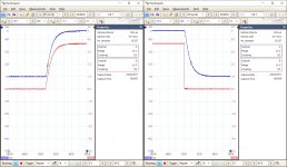
Back to this one, traces are attached. Yes D7 bias (red trace) is either floating or held low. The gate (blue) shows the PWM network filter shaping. So I'm not sure what can be done software wise. It is making me wonder how an external DAC would perform.
Took the time out to go to one of the UKs largest hifi shows in a hotel so each room was like a mini test setup with loads of manufactures. Also met one of the Mark's behind Mark Audio wihich was good as I have just purchased a pair of Alpair 7Ps. These are currently on thier 100hour run-in period being driven by my recently (almost) finished Modulus-86 build. On the way there I picked up some pre-cut panels for a frugal horn. So as you can see there are a few projects on the go at the moment.
Back to this one, traces are attached. Yes D7 bias (red trace) is either floating or held low. The gate (blue) shows the PWM network filter shaping. So I'm not sure what can be done software wise. It is making me wonder how an external DAC would perform.
Attachments
5LN01C might also become obsolete soon, so I was looking for alternatives. This one might be it:
https://www.fairchildsemi.com/datasheets/FD/FDV301N.pdf
I am also having problems with the Mosfet. I see that you used the above mounted on a heat sink ? I assume that whiteout heat-sink there will be fluctuations in the Vgs, but still the feedback circuit should take care of those..
I am also having problems with the Mosfet. I see that you used the above mounted on a heat sink ? I assume that whiteout heat-sink there will be fluctuations in the Vgs, but still the feedback circuit should take care of those..
It's not the heatsink, it's homemade pcb SOT23 adapter 😉
I am using a 3ln01c sot23 mosfet (directly on PCB) but with a different design. While measuring the LDRs resistance I get a 1.5 to 2% skew (from calibrated resistance) after a while , with the same Vgs .If I place a fan next to board the skew drops to 0.5% I assume that photo-resistors of LDR have a thermal skew independent of LED (Vgs and Vdf)
Have you seen this before ?
Have you seen this before ?
Its not about the FETs, its that photo resistor changes R depending on the ambient temp.
First I calibrate at room temp and 45 min after the PCB heats up an extra 14C and LDR about 6C. When I do the measurements the LDR resistance changes about 2-4.5% from initial calibrations (and we can see the Vgs/Vgf is same value as in calibration)...only change is the photoresistor heating up.
I assume its not so bad since all LDRs will heat and change the resistance almost linearly ( check datasheet of another Cds photocell) so channel skew will be minimal.
I was trying to get a precision of 0.5% or 0.1%. Because of the temp skew that seems to be out of reach.
Been off finishing my speaker build. Now they are done and coupled to the amp I need a pre-amp so back to this.
I'll start by saying I'm no design engineer or programmer but I was wondering if using an external I2C DAC might be a better bet than using PWM. With the increased resolution and the lack of RC filters it might mean we can get rid of the middle bump. There are loads to chose from but this seems like a good start... MCP4728. There is enough current on the outputs so that the LDR LEDscould be driven directly so may simplify the build ultimatley.
Given the thermal drift of the LDRs I'm also thinking they might benifit from being thermally coupled to each other. An ali bar with 4 suitable dia holes for the LDRs to be slid into with bit of heatsink paste could work quite well?
- Home
- Source & Line
- Analog Line Level
- Arduino based LDR volume and source selection controller