At frequencies at which there are many other practical things to worry about (wiring, capacitors ESL, parasitic capacitances, etc...).
Exactly so. This means the simulated 12 dB GM, which is just adequate, is almost certainly worse in practice and probably not really adequate. So the loss of 6 dB is of practical importance after all.
Am I correct that you never posted the schematic for which you got those plots for?...
The schematics were posted and I included a link to them. It's a few posts further on.
I would be curious to analyze that zero that, it seem not to be due to Miller. That's because it's at a frequency that's much lower than a common Miller loop ULGF.
Yes, I also considered it curious, that's why I posted it. I suspect it is due to the feed-forward zero but as I stated earlier, it is not obvious and I never looked at the inner loop. That would be of interest and I look forward to your conclusions.
Best wishes
David
Last edited:
The schematics were posted and I included a link to them. It's a few posts further on.
That's essentially a Blameless, but with 8 bipolar output pairs I wonder how you got an ULGF > 1MHz.
Please post the .asc file with any specific changes for that schematic.
It would be helpful if you could point out the relevant components implementing this in your schematic.I think that Inclusive Output Compensation, in this case in combination with shunt compensation,
but looks very stable at least in the simulation.
BR Damir
That, unfortunately, is a long way from conclusive
I agree Edmond, the 'thermal' way doesn't get that far. In my tests I went from heaksink-mounted TO-3 to 'air-mounted' TO-247 and the difference is very small - in each case you see the thermal delay from dissipation even to the diode on the ThermalTrak devices. Not sure I understand the exact mechanism though.
OTOH, with a few % transient shift in bias, should we worry anyway?
Jan
I suspect the answer is that at these subsonic frequencies the global NFB is maximal and that covers up a multitude of thermal sins. The single-ended EF VAS gives an o/l gain of about +117 dB at 10 Hz, leading to an NFB factor of 90 dB with the usual c/l gain. Perhaps significantly, a push-pull VAS gives some 40 dB less o/l gain, and would be much worse at dealing with subsonic shenanigans.
The push-pull VAS approach certainly does seem to have a lot of flaws.
That's essentially a Blameless, but with 8 bipolar output pairs I wonder how you got an ULGF > 1MHz.
The drivers are fairly fast, 100MHz and lowish capacitance rather than the usual slow stuff. Careful optimization of other details, compensation, PCB layout etc. Not mine but I believe it's accurate.
Please post the .asc file with any specific changes for that schematic.
Best wishes
David
Found it.
Attachments
Last edited:
Compensation tweeking Drama --
Jeeeez guys..... If the open loop BW was much much greater than a super high gain amp usually has...... these issues would be put far away from audio and easily compensated without Any affect on the amp stability or closed-loop stability etc. etc. etc.
The idea or terminology used to say that a certain compensation reduces high freq distortion is fundemantally because of the phase shift created allowes for more NFB to be applied.
It has been shown that other topologies can also produce extremely low THD/IM without all the drama of compensation tweeking.... [which is killed when going from SIM to build in many cases].
D.Self has done a fine job of describing, in detail, a certain single topology and what he likes about it. Anyone applying distortion cancellation in amplifiers? This example isn't an amplifier -- buffer-- but along more interesting lines.... how could it be made into an amplifying stage and keep the cancellation working?? Google - Quadlotron.

THx-RNMarsh
Jeeeez guys..... If the open loop BW was much much greater than a super high gain amp usually has...... these issues would be put far away from audio and easily compensated without Any affect on the amp stability or closed-loop stability etc. etc. etc.
The idea or terminology used to say that a certain compensation reduces high freq distortion is fundemantally because of the phase shift created allowes for more NFB to be applied.
It has been shown that other topologies can also produce extremely low THD/IM without all the drama of compensation tweeking.... [which is killed when going from SIM to build in many cases].
D.Self has done a fine job of describing, in detail, a certain single topology and what he likes about it. Anyone applying distortion cancellation in amplifiers? This example isn't an amplifier -- buffer-- but along more interesting lines.... how could it be made into an amplifying stage and keep the cancellation working?? Google - Quadlotron.
THx-RNMarsh
Last edited:
The drivers are fairly fast, 100MHz and lowish capacitance rather than the usual slow stuff. Careful optimization of other details, compensation, PCB layout etc. Not mine but I believe it's accurate
I'll check it out in detail, but speaking about a practical view: two 1A 2SC4793/2SA1837 driving 8 pairs of 2SC5200/2SA1943 at +/-70V is a joke from a drivers SOA and even max current perspective. You need much stiffer drivers (like another pair of 2SC5200/2SA1943) and then there goes your high ULGF.
Jeeeez guys..... If the open loop BW was much much greater than a super high gain amp usually has...... these issues would be put far away from audio and easily compensated without Any affect on the amp stability or closed-loop stability etc. etc. etc.
We are talking power amplifiers here, Mr. Marsh.
It would be helpful if you could point out the relevant components implementing this in your schematic.
Output Inclusive Compensation (OIC) , output via C12 and C9, C10 to the VAS input.
Shunt C17 and R38.
That, unfortunately, is a long way from conclusive
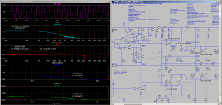
Phase margin of 70 degree and Gain Margin of 41 dB looks stable to me.
Best regards
Damir
Attachments
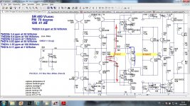
C17 looks far too small to implement shunt compensation, though it might be useful against parasitics. When I replaced a 100 pF Miller capacitor, I needed 44 nF of shunt capacitance to get the same o/l gain roll-off. That was using a single-ended VAS, but I doubt if the properties of the circuit we are discussing here are that radically different.Output Inclusive Compensation (OIC) , output via C12 and C9, C10 to the VAS input.
Shunt C17 and R38.
Phase margin of 70 degree and Gain Margin of 41 dB looks stable to me.
Damir
Yes, but it is only a simulation. Have you actually built that design?
We are talking power amplifiers here, Mr. Marsh.
So am i... just extend the concept to a power amp rather than a literal interpretation. It was an illustration of a topology which uses cancellation to reduce distortion.
Cant we get away from this now "standard" - albeit excellent topology- being discussed from the book - The compensation of the "standard" topology has been written about for a long time and we are still arguing about how it works and what it does, exactly.
I made a point about other toplogies dont have all this compensation tweeking for low distortion and stability behaviour issues that this topology has... or not to the same extent re. audio.
If anything, I understand this is about the author's chosen design.... the compensation of it is the Achille's Heel of the designs as far as DIY'ers are concerned (IMO). I complained about the design of Bob Cordell's for the same reason.
-RNM
Last edited:
I made a point about other toplogies dont have all this compensation tweeking and stability behaviour issues that this topology has... or not to the same extent re. audio.
If anything, I understand this is about the author's chosen design.... the compensation of it is the Achille's Heel of the design as far as DIY'ers are concerned (IMO).
-RNM
Well, that's news to me.
Follow a few simple rules and the stability is bulletproof. (Mr Creevy)
Do remember I have built thousands upon thousands of these.
Well, that's news to me.
Follow a few simple rules and the stability is bulletproof. (Mr Creevy)
Do remember I have built thousands upon thousands of these.
I understand..... and many other makes, models and brands have been using similar designs for a long time and are stable, also. This forum however, makes it seem like a difficult task without sophisicated testing and SIM and great insight into circuit behavior.
Please give us/me the place and point where simple equations will yield low distortion and stable operation, again.
THx-RNMarsh
C17 looks far too small to implement shunt compensation, though it might be useful against parasitics. When I replaced a 100 pF Miller capacitor, I needed 44 nF of shunt capacitance to get the same o/l gain roll-off. That was using a single-ended VAS, but I doubt if the properties of the circuit we are discussing here are that radically different.
OK, I would say that C17 and R38 help the main OIC to get better Bode plot.
I did not simulate VAS output impedance, but it looks that it is quite high.
Yes, but it is only a simulation. Have you actually built that design?
Yes this is only simulation, I did not built it yet, but I am quite confident in the simulation result.
I have built my TT TMC amp(showed some pages earlier) and simulated values were very accurate, amp is stable and in use for two years now.
OIC
In the past we have already discussed this matter. Now you are giving the same answer again. C17 (together with R38) is not meant as a replacement of the traditional Miller compensation cap and is not meant to stabilize the global FB loop (as for the latter, these caps are located elsewhere). Instead, the purpose of C17 is to stabilize the Miller loop itself. Obviously, the value of this shunt capacitor should be much much lower and certainly not a huge 44nF.
Cheers, E.
Dear Mr Self,C17 looks far too small to implement shunt compensation, though it might be useful against parasitics. When I replaced a 100 pF Miller capacitor, I needed 44 nF of shunt capacitance to get the same o/l gain roll-off. That was using a single-ended VAS, but I doubt if the properties of the circuit we are discussing here are that radically different.
[..]
In the past we have already discussed this matter. Now you are giving the same answer again. C17 (together with R38) is not meant as a replacement of the traditional Miller compensation cap and is not meant to stabilize the global FB loop (as for the latter, these caps are located elsewhere). Instead, the purpose of C17 is to stabilize the Miller loop itself. Obviously, the value of this shunt capacitor should be much much lower and certainly not a huge 44nF.
Cheers, E.
What I am thinking about is more along the lines of when compensation is Not used Only for stability. Rather, when it is used for two functions -- stability and lowering HF THD. That is where the great amount of tweeking or finessing is needed -- esp after the build. That it can be done with some knowledge of the art for consistent, stable production isnt the matter for me. It is the part of compensation that is used for double duty..... other topologies can use compensation Only for stability and not for HF distortion reduction. The distortion can be reduced other ways without the compensation also being involved in distortion reduction.
[I am ignoring the distortion due to excessive loading/currents caused by compensation C]
THx-RNMarsh
[I am ignoring the distortion due to excessive loading/currents caused by compensation C]
THx-RNMarsh
Last edited:
More schematics :Adrian-Kingston.com - Technics SE-A5
Joachim I was thinking along the lines of SAE 5000 series, these have a more complex vas and probably lower distortion than the example you posted. I didnt find figures for SAE 5.
I'll check it out in detail, but speaking about a practical view: two 1A 2SC4793/2SA1837 driving 8 pairs of 2SC5200/2SA1943 at +/-70V is a joke from a drivers SOA and even max current perspective. You need much stiffer drivers (like another pair of 2SC5200/2SA1943) and then there goes your high ULGF.
Attached the joke driving 2.1R during heavy overload just before current limit starts. The PSU would not be able to deliver such high currents.
Br, Toni
Attachments
Last edited:
- Status
- Not open for further replies.
- Home
- Amplifiers
- Solid State
- Your opinions are sought on Audio Power Amplifier Design: 6th Edition. Douglas Self