Hi Scott,
I don't know what to say to you at this point. I have never had to do anything like this to one of these amplifiers.
With everything connected as in factory condition, a high DC offset usually means that you have some conductive capacitor dielectric still on / in the board, and possibly on some components. This stuff is really difficult to deal with and drive you nuts to solve through troubleshooting.
The reason this fluid doesn't follow normal troubleshooting procedures is that with troubleshooting, you are looking for a defective component(s). You don't consider the circuit board as being defective, and you need to include that scenario in your thinking.
-Chris
With everything connected as in factory condition, a high DC offset usually means that you have some conductive capacitor dielectric still on / in the board, and possibly on some components. This stuff is really difficult to deal with and drive you nuts to solve through troubleshooting.
I think I have the DC offset under control at this stage. With the OpAmp disconnected I can set it to near zero (2-3 mV), and with the servo in place, it stays put over time.
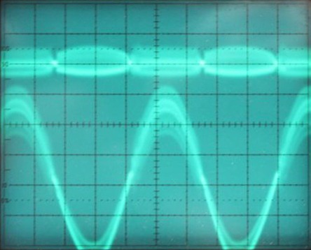
My current issue is actually a low level oscillation. It is fixed in amplitude (about 100-300 mV), and seems to be related to the input signal. At the zero crossing of the input there is no oscillation, and at the peaks (positive or negative) it it at its peak. It is very high in frequency.
I see it in the output signal, on the supply lines and also at the input of the amp. It goes away when I turn off the amp, or if I turn off the signal generator creating the input signal. I am not sure if it is the amp by itself reacting to the input signal, or some weird interaction between the signal generator and the amp.
Here are some pics.
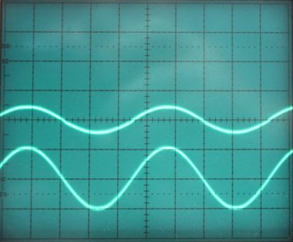
Input signal with the amp off. The top trace is the amp output, and the bottom is the input signal at 1 volt/division
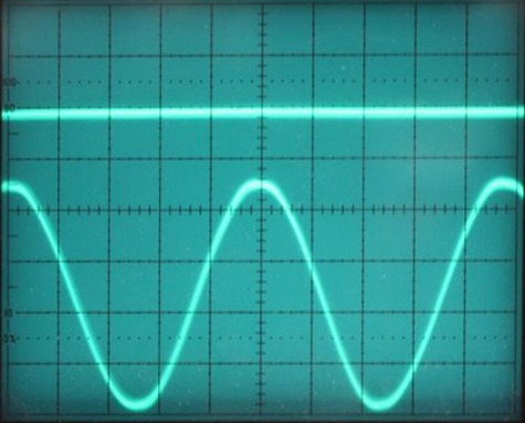
High signal level. Top trace is the output at 50 volts/division (into 8 ohms), bottom signal is the input at 0.5 volt/division.
Here are the input and output at a lower signal level The bottom trace is the input signal at 0.2 volt/div. The top is the output signal (forgot the scale).
Obviously something odd going on here.
Here is same input signal (bottom) and the positive rail at the big filter cap (at 0.1 volt/div)
And here is the ground at the same cap.
This oscillation only occurs when the output stages are connected. If I run the control board open loop wight he leads tot he output stages shunted by resistors (680 ohms), I get nice big clean signals.
I am thinking this is either something in the output stage, or possibly some parasitic oscillation in the rectifier. I changed the rectifier, but I have not tried shunting the legs with an RC circuit.
As you can see, the frequency is very high (for reference, the input signal is 1KHz), and that actually may point to rectifier oscillation. Under lighter load, the rectifier may not do this, or may not do it as much.
I suppose one thing I could try would be to apply a low DC voltage to the input, on the other side of the blocking cap, and see if it oscillated with any sort of signal level. That would also tell me if this was some weird interaction between the amp and my signal generator. It is possible that the amp is somehow feeding signal over the AC lines to the signal generator and causing it to oscillate...
Scott
Last edited:
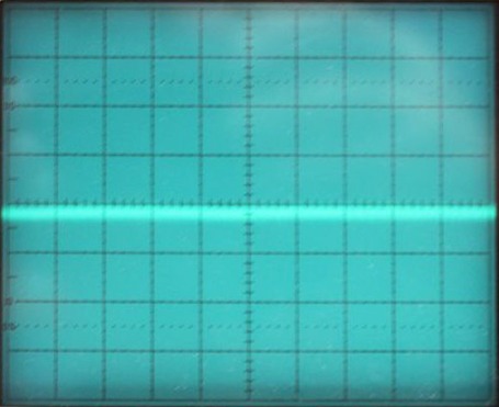
Here are a few additional traces, this time with no input signal.
This is the output of the amp DC coupled to the scope at 20 mV per division. You can see there is about 2-3 mV of negative DC offset. You can also see (at least I could on the live scope) a very low level oscillation.
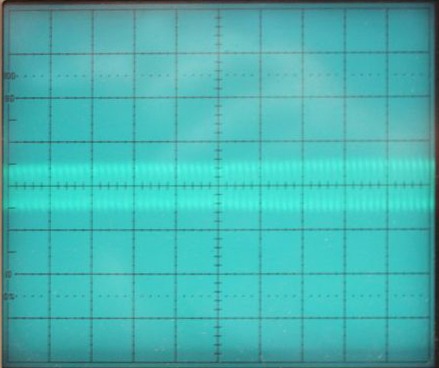
You can see this better in this pic. This is the output at 20mV/div with nothing attached to the input. Same low level oscillation as above, but larger.
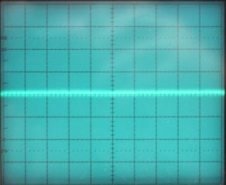
And here is the output at the same scale, with the input grounded.
Scott
This is the output of the amp DC coupled to the scope at 20 mV per division. You can see there is about 2-3 mV of negative DC offset. You can also see (at least I could on the live scope) a very low level oscillation.
You can see this better in this pic. This is the output at 20mV/div with nothing attached to the input. Same low level oscillation as above, but larger.
And here is the output at the same scale, with the input grounded.
Scott
Hi Scott,
Basically, when you have oscillation, it will show up everywhere. At those high frequencies, the filter capacitors are open circuit. Check the small capacitors that act as filters on the power supplies. Also check / replace the electrolytic capacitors on the output boards. Make absolutely certain the heat sinks are both securely grounded - a low resistance connection to the main chassis.
Are the output transistors the original parts? If not, you may have to adjust the compensation capacitor across the feedback resistor.
-Chris
Edit: Nice 'scope screen shots. How are you doing this?
All good suggestions. I plan to go around the amp next and make certain everything is grounded properly. I'll also replace the caps and resistors on the small boards on top of the big filter caps.
I just determined, however, that the high frequency load resistor (R158) on the control board appears to be open. Seems like that's probably the culprit. According to the manual R158 and C121 (it looks like a typo, since is says C111, but that is unrelated) "provide a load for the amplifier at high frequencies". If that were open, then there would-be no high frequency load and the amplifier would probably be unstable.
So, back to Mouser for the umpteenth time!
Cheers,
S
Well, OK then.. The Adcom is finally working.
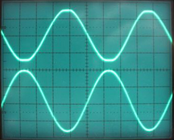
I replaced R158, the 3 watt resistor that provides a load to the amp at high frequencies (about 300 KHz). The original one was open circuited. That one took a little head scratching to home in on...That killed most of the oscillation. The rest was due to some bias errors that were a result of me tweaking the bias to try to manage the high frequency oscillation. Once I put in the replacement load resistor, I spent a little time little tweaking the diff amp currents, and the oscillations stopped. The result was the signal traces below.
The currents in the diff amps are running about 1.4 mA each leg. They could be better balanced, each leg is running about 0.3 mA different than the other leg. I'll go through that matching process again, and see if I can do better. .
The output offset is about 40 mVolts, which seems good, and it is very stable
Here are the traces:
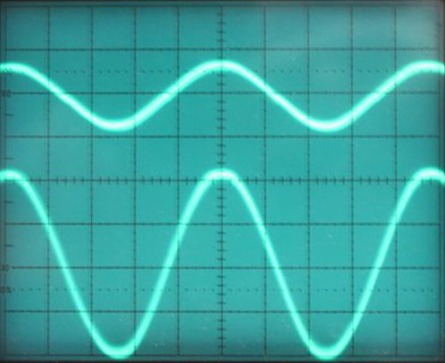
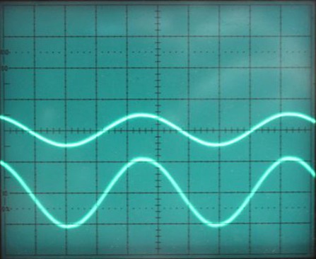
This is 1KHz around half rated input level into 8 ohms.
The bottom trace is the input signal at 1 volt/division. The top trace is the output at 50 volts/div. The output peak signal here looks to be about 25 volts, so that's about 80 watts into 8 ohms. I can run it hotter, but until I am sure everything is OK, I'd rather not push my luck!
This trace is at 0.1 volts/div on the input, and 5 volts/div on the output, so about 10 dBV lower input signal level.
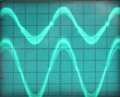
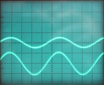
This is the same scope and input settings as above, only at 10 KHz...
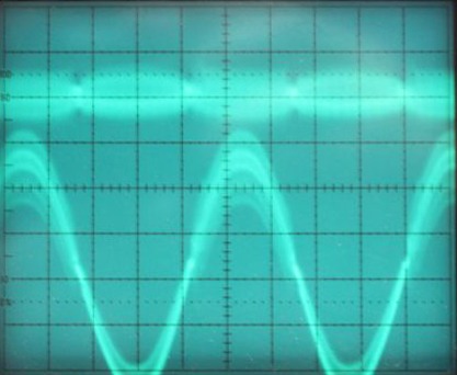
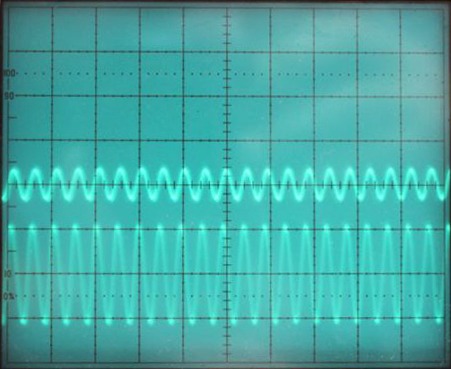
And, just for kicks, this is how it performs at 100KHz.. Dayumn!!
So, it has been a long hard road, but I think I have finally reached the end of it.
This amp had multiple issues when I got it. Fortunately I paid very little for it. I probably have about $250 in parts in it now (including a big pile for the big filter caps), but it seems to be stable and working very well. Now that I know the currents that work for the current sources, I'll probably measure my current source resistors and put in fixed resistors.
To catalog its ills:
1. It had the well-known electrolyte issue. I found a good scrubbing with CRC 'Lectraclean, and Also CRC Air Intake cleaner (both very macho hydrocarbon cocktails) did a great job on the boards (see earlier posts for some pics of this).
2. It had multiple failed transistors, several bad dies and a couple of fried or otherwise open resistors. This made troubleshooting difficult, because until I managed to find all of the bad parts, it didn't work, and often replacing one bad part didn't work, because it had failed because of some other problem (like replacing blow fuse without fixing the short...)
3. There were several loopy "fixes" from some PO. There were those weird trim pots in place of the 1K load resistors on the diff pairs. not sure what the logic was behind those.
4. There were some quirky diode replacements. I went by the data sheets on the diodes, and found that in many cases the new replacements from Mouser and/or Dgikey did not match the data sheets (in terms of forward voltage drop). I actually need up with LEDs for one set of diodes (beyond the ones in the current sources), because these has the correct forward drop. The voltage drop on the diodes is critical to the proper bias set up of the driver stages. I suspect this is the key issue in most repairs (other than the electrolyte problem). If you just replace the diode and varistors with supposedly compatible parts, it may not work. SO pay special attention to the voltage drops, and check the parts you put in to be sure they perform correctly (vs just have the right numbering).
I now need to button it up, and install my cool fan arrangement.
I'd like to thank Chris (Anatech) for his super helpful advice as I went through this. I would have quit somewhere along the way if he had not been there to offer good advice. What a wonderful resource!
One of these days I'll write up the operational concept for this amplifier in more detail, since I found it very helpful to understand how it was supposed to work when trying to figure out why it wasn't working.. I'll also post a few pics of what the various signals are supposed to look like when it is working properly so others don;t need to bumble around in the dark like I did.
Cheers everyone!!
Scott
I replaced R158, the 3 watt resistor that provides a load to the amp at high frequencies (about 300 KHz). The original one was open circuited. That one took a little head scratching to home in on...That killed most of the oscillation. The rest was due to some bias errors that were a result of me tweaking the bias to try to manage the high frequency oscillation. Once I put in the replacement load resistor, I spent a little time little tweaking the diff amp currents, and the oscillations stopped. The result was the signal traces below.
The currents in the diff amps are running about 1.4 mA each leg. They could be better balanced, each leg is running about 0.3 mA different than the other leg. I'll go through that matching process again, and see if I can do better. .
The output offset is about 40 mVolts, which seems good, and it is very stable
Here are the traces:
This is 1KHz around half rated input level into 8 ohms.
The bottom trace is the input signal at 1 volt/division. The top trace is the output at 50 volts/div. The output peak signal here looks to be about 25 volts, so that's about 80 watts into 8 ohms. I can run it hotter, but until I am sure everything is OK, I'd rather not push my luck!
This trace is at 0.1 volts/div on the input, and 5 volts/div on the output, so about 10 dBV lower input signal level.
This is the same scope and input settings as above, only at 10 KHz...
And, just for kicks, this is how it performs at 100KHz.. Dayumn!!
So, it has been a long hard road, but I think I have finally reached the end of it.
This amp had multiple issues when I got it. Fortunately I paid very little for it. I probably have about $250 in parts in it now (including a big pile for the big filter caps), but it seems to be stable and working very well. Now that I know the currents that work for the current sources, I'll probably measure my current source resistors and put in fixed resistors.
To catalog its ills:
1. It had the well-known electrolyte issue. I found a good scrubbing with CRC 'Lectraclean, and Also CRC Air Intake cleaner (both very macho hydrocarbon cocktails) did a great job on the boards (see earlier posts for some pics of this).
2. It had multiple failed transistors, several bad dies and a couple of fried or otherwise open resistors. This made troubleshooting difficult, because until I managed to find all of the bad parts, it didn't work, and often replacing one bad part didn't work, because it had failed because of some other problem (like replacing blow fuse without fixing the short...)
3. There were several loopy "fixes" from some PO. There were those weird trim pots in place of the 1K load resistors on the diff pairs. not sure what the logic was behind those.
4. There were some quirky diode replacements. I went by the data sheets on the diodes, and found that in many cases the new replacements from Mouser and/or Dgikey did not match the data sheets (in terms of forward voltage drop). I actually need up with LEDs for one set of diodes (beyond the ones in the current sources), because these has the correct forward drop. The voltage drop on the diodes is critical to the proper bias set up of the driver stages. I suspect this is the key issue in most repairs (other than the electrolyte problem). If you just replace the diode and varistors with supposedly compatible parts, it may not work. SO pay special attention to the voltage drops, and check the parts you put in to be sure they perform correctly (vs just have the right numbering).
I now need to button it up, and install my cool fan arrangement.
I'd like to thank Chris (Anatech) for his super helpful advice as I went through this. I would have quit somewhere along the way if he had not been there to offer good advice. What a wonderful resource!
One of these days I'll write up the operational concept for this amplifier in more detail, since I found it very helpful to understand how it was supposed to work when trying to figure out why it wasn't working.. I'll also post a few pics of what the various signals are supposed to look like when it is working properly so others don;t need to bumble around in the dark like I did.
Cheers everyone!!
Scott
Last edited:
Hi Scott,
Thank you for your kind words. You stuck with a difficult repair and saw it through to a successful completion. Many others would have given up.
As soon as you found the open zobel network, I knew that the amp would work as designed. The original repair attempt before you got it really didn't help you from a troubleshooting standpoint.
I guess the one thing you can learn from this is that equipment from a good group of designers will always work as designed. There are many of these amplifiers out there that run well as they were designed. The difficult thing to decipher is which equipment is well designed, and which brands are actually running on the edge of destruction as designed. There are many examples of this out on the market. It doesn't make the job of a technician any easier, and that's for sure.
I think you did an excellent job, especially considering the state the amp was in when you received it.
-Chris
Thanks Chris.
This was an interesting and educational project for me. I have a graduate degree in EE, but it has been decades since I did any significant circuit design, or troubleshooting. It was good to get back into it, and to use some theoretical skills to figure out what I should be seeing vs what I was seeing, and from that deduce why I was seeing that. I think the core issue, all said and done, was the wrong voltages in the diode stack that biases the driver circuit...Once I got that right, and had the current sources correctly set, it all basically worked.
One thing I was really impressed with is the DC coupled design of this amp. This is a very high powered piece of equipment, and the design takes the AC input signal all the way from a zero DC offset to 83 volts or so, and then moves it down from there, while amplifying the AC signal, all the way back to two slightly offset signals to drive the output in class AB. Very clever and very elegant.
The basic operational state of this amp revolves around the biasing scheme. If the currents in the input diff pair are wrong, then two problems arise:
1) The voltage offset at the collectors of Q103/Q104 will be off, and;
2) If the collector voltage at Q103/Q104 (or the bases of Q109/Q110), which depends on the currents in 1), are not properly suited to the diode tree voltage drops (D103, D105, and D107), then the driver stages will be off.
3) If the positive and negative side diff amps are are unbalanced, then the output offset voltage will rise..The servo can compensate for this to some degree.
From what I was able to see first hand, elements 2 and 3 above are the critical issue when the output offset is high (like railed). Once the bias stacks are off, then the big power drivers get unbalanced, and signals get really offset (20-40 volts).. that propagates into the output and you have a mess. Not only do you get a huge DC offset, but the waveforms may clip in one direction or the other as well.
Two areas I still do not fully understand are the driver output bias network, and the oddball distortion sensing circuit....the one that seems intermingled with the servo feedback network...but, I guess we need to always have SOME mystery in our lives!
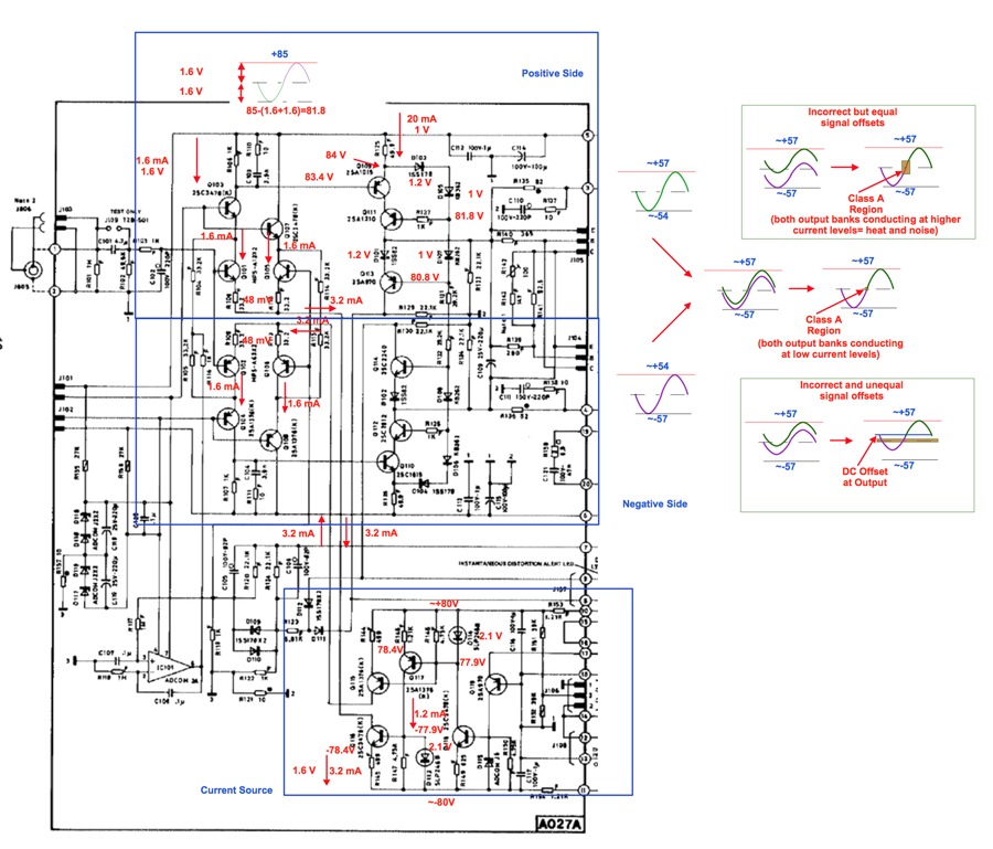
As promised, here's a quick tour of the Adcom GFA565...
Looking at the diagram of the control board below. we see in the lower right portion of the circuit the current sources. This circuit is similar to the Darlington matching circuit posted by Anatech. The current through either of the LEDs creates a stable voltage drop of about 2. 1 volts, and that turns on a transistor which then has a fixed base emitter drop. That drop essentially propagates the LED voltage (shifted by the base emitter voltage of the transistor) to the transistor's emitter resistor. The value of this resistor and the applied voltage then result in the 3.2 mA current. Since these are fixed, and independent of the collector side of the transistor, the current is fixed at 3.2 mA. If the load changes, the collector voltage will change accordingly in order to maintain 3.2 mA.
This current is then split between the differential pairs (the MPSA13, and MPSA63 Darlington pairs, Q101/105 and Q102/106), so each leg draws 1.6 mA.
The 1.6 ma current in, for example the Q101 leg then gets pulled across the 1K load resistor (R106), thereby dropping 1.6 volts. Since the other side of this resistor is at the positive rail, the voltage at the collector of Q103 is then 83.4 V (=85-1.6). The same thing happens on the negative side (Q102/106).. except the voltages are negative.
I have also drawn in what the AC signal would ooh like here. When the input voltage at Q101 is at its max value, the transistor is most of the way on, and when it s at its min value, it is mostly off. When it is off, the current in that leg of the diff pair is low, and the current in the other side (in this case Q105 is high.. so they swap the 3.2 mA back and forth over the cycle of the input signal swing). When the current in the Q101 leg is low, the voltage drop across R106 (the 1K resistor) is low, so the voltage on the base of Q109 is close tot he rail voltage. on the other half cycle, the Q101 leg is drawing most of the 3.2 mA and the voltage drop across the load is at it maximum, and the voltage at the base of Q109 is about 81.8 volts. The maximum swing here is this +/- 1.6 volts, or 3.2 volts peak to peak. As noted above, the zero input (quiescent, or bias voltage is 83.4).
R106 is also connected to the base of Q109, so with no AC signal input, the base is also at 83.4 volts. Since the base emitter drop is about 0.6 volts, the emitter of Q109 is at 84 volts. Q109 is a PNP transistor, so things in this circuit are referenced to the positive rail as opposed to the more usual situation where the emitter is grounded and the load is on the positive rail.
With 84 volts at the emitter of Q109, this means that the voltage drop across R125 is 1 volt. R125 is 49.9 ohms, so using Ohm's law we get a current of 20 mA through tat resistor and thus through Q109 (20 mA=.020=1/49.9). This is the bias current for Q109 and Q111. Now the fun begins...
A small portion of this 20 mA current splits off and cascades down the diode stack formed by D103, D105 and D107. These have fairly stable forward voltage drops. So, the pair of diodes D103 and D105 drop about 2.2 volts to set the base voltage of Q111 at about 81.8 V.
As noted above, over the AC signal swing, the base of Q109 goes from about 85 (rail) to 81.8 volts. At 85 volts there is very little current flowing in Q109 and Q111,so the collector of Q111 is nominally zero volts. Remember, disregarding the output banks, the collector here is connected to ground by R133. So with little or no current, the voltage here (disregarding the negative side of the amplifier for a moment) would be at or close to zero. In fact, however, since the collector of Q111 is also connected to the NEGATIVE side of the amplifier through R139 and the series/parallel network of R141, R142 and the R143 trimmer pot (the messy little network on the upper right side of the diagram), AND since when the positive side of this system is nearly off, the negative side is nearly all the way on, the voltage at the collector of Q111 gets pulled down to nearly the negative rail. During the other half cycle of the input signal, the base of Q109 is at its lowest voltage (81.8 V), and Q109 and Q111 are fully on. Singe the voltage swings are symmetrical, this puts the peak current through Q111 at about 40 mA. Remembering that at this point in the signal cycle the negative side os mostly off, the voltage at the collector of Q111 rises. The peak value is about 50 volts or so.
The result of this back and forth between the positive and negative cycles is that the signal at terminal 3 swings from about +57 volts to -54 volts, and the voltage on terminal 4 swings from about +54 volts to about -57 volts. These signals are in phase, but offset relative to one another by about 3 volts. (it is instructive (with the output stages disconnected) to put a pair of resistors across terminals 3 and 4 with the connection between them grounded. If you view the signals on a scope, they will look like the sketch I have provided (if you do this, remember that wight he output disconnected there is no feedback, so the gain is really high, and you need to reduce the input AC signal level by about 10:1).
So, at this stage we have some very high voltage signals, but relatively little current capacity.
These big, slightly offset signals are then applied to the output stages.
The output stages are what is known as a "triple Darlington". For those who are not familiar with this, a Darlington is a configuration where the emitter of one transistor feeds directly into the base of another, and the collectors are tied together. Since the collector-emitter current of the first transistor is fed directly into the base-emitter junction of the second transistor, the collector emitter current in the second transistor is multiplied up...a lot. If the current gain of each transistor is 100, the current gail of a darlington configuration is 10,000 (=100 x100). A triple darlington is thus this game played three times, so the current gain is more like 1,000,000. To support this high current, the output stages are basically a single darlington pair that then feeds a whole bunch of power transistors all basically connected in parallel (there is a bit more to it than this, but you get the idea).
In order to generate 300 watts RMS across 8 ohms, we need to generate 1.41 times that at the peak (the difference between peak and RMS),so the output voltage swing must be about +/-57 volts. That yields a peak current of E/R=57/8=7.125 Amps. As the signal passes from one half cycle to the next, there is a slight overlap between the two output banks, meaning that they are both conducting. This means that some current is actually flowing between the output banks and not through the load, but this current is relatively small because the voltage levels are small, and passing through zero. This overlap avoids the situation where both banks are off,causing a small flat spot at the zero cross in (known as "crossover distortion"). This is the core difference between a class B "push-pull" amplifier, and this "Class AB" amplifier.
So, that's pretty much the signal path and operation of the amp.
I have also shown in the figure two fault conditions that can arise in this amp. in the upper right side I show a situation where the positive and negative driver signals are offset in equal but opposite directions. The result of this is that the amp is in Class A (both banks conducting) over more of the signal cycle. This consumes a lot of power, since the banks are basically conducting higher current straight through from one bank to the other. My amp had this issue. When I bought it, the guy who sold it said "it hums". I though it had the 60 cycle hum typical of bad filter caps. No such luck. What he meant was that it physically hummed. When the output stages were connected the giant port transformer would buzz like a neon sign, the heat sinks would get hot, and the lights would dim a little.. YIKES!!!
The other situation is more typical Here the driver signals are offset in the same direction. This basically results in a DC offset at zero input.
Both of these situations can arise from the bias diode stacks being screwed up, or from the current sources being unbalanced. These two things play against each other as well, yielding some challenges when troubleshooting things.
Cheers,
Scott
A final wrap up (at least until I open up my other GFA 565...).
I measured the current source pots as set for the performance in the pics above. They were within about 10% of the fixed resistor values on the schematic (one high, the other low). I replaced them with the proper 499 ohm resistors, and tested that. There was still a hint of oscillation, especially right after it was turned on. I traced this to the C103 and C104 filter caps that bypass the input stage load resistors (R106 and R107). After some fiddling, I tried a 10K pf cap instead of the 3800 pf cap. Worked like a charm!
I still had some lower frequency fuzz on the waveform, and I noticed that this changed when I touched the heat sinks, or covered the open unit with my hand.. So, I figured it was time to button the old girl up.. (I recall Chris had said that it was necessary to ground the heat sinks. I think this oscillation is what he was referring to. It looked to be around 100KHz...). I re-installed the control board, dressed the wires a bit, and replaced one of the 8.2K 2 watt resistors on the filter cap boards (I had noticed that the positive supply took about 5X longer to discharge than the negative supply, so I figured it might be the discharging resistor...). I put the top cover on, and replaced all the screws.
Here are the traces now. MUCH BETTER!!!
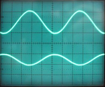
This one is a full rated power. The bottom trace is the input (2 volts/div), and the top is the output (50 volts/div). You can see that the amp is just starting to clip.
Here are the traces at my signaL generator's lowest signal level. Bottom is the input (.1 volt/div, top is the output at 2 volts/div.
I think it is working properly now. Time to connect it up to my system!!
Cheers,
Scott
I measured the current source pots as set for the performance in the pics above. They were within about 10% of the fixed resistor values on the schematic (one high, the other low). I replaced them with the proper 499 ohm resistors, and tested that. There was still a hint of oscillation, especially right after it was turned on. I traced this to the C103 and C104 filter caps that bypass the input stage load resistors (R106 and R107). After some fiddling, I tried a 10K pf cap instead of the 3800 pf cap. Worked like a charm!
I still had some lower frequency fuzz on the waveform, and I noticed that this changed when I touched the heat sinks, or covered the open unit with my hand.. So, I figured it was time to button the old girl up.. (I recall Chris had said that it was necessary to ground the heat sinks. I think this oscillation is what he was referring to. It looked to be around 100KHz...). I re-installed the control board, dressed the wires a bit, and replaced one of the 8.2K 2 watt resistors on the filter cap boards (I had noticed that the positive supply took about 5X longer to discharge than the negative supply, so I figured it might be the discharging resistor...). I put the top cover on, and replaced all the screws.
Here are the traces now. MUCH BETTER!!!
This one is a full rated power. The bottom trace is the input (2 volts/div), and the top is the output (50 volts/div). You can see that the amp is just starting to clip.
Here are the traces at my signaL generator's lowest signal level. Bottom is the input (.1 volt/div, top is the output at 2 volts/div.
I think it is working properly now. Time to connect it up to my system!!
Cheers,
Scott
Thanks Chris.
The trace in the pic above shows the output signal at about 75 volts peak..That's 75 volts across 8 ohms, or.. hold on to your hat..497 watts rms!!!! (75*75)/8=703, and 703*.7071=497...
Yikes!! This thing is a beast!!
Scott
The trace in the pic above shows the output signal at about 75 volts peak..That's 75 volts across 8 ohms, or.. hold on to your hat..497 watts rms!!!! (75*75)/8=703, and 703*.7071=497...
Yikes!! This thing is a beast!!
Scott
Hi Scott,
Are you measuring voltage peak to peak? If so, divide by 2 and multiply that buy 0.7071 (approx) to get the steady state rms power.
-Chris
Are you measuring voltage peak to peak? If so, divide by 2 and multiply that buy 0.7071 (approx) to get the steady state rms power.
-Chris
No, the image shows 75 volts peak, 150 volts peak to peak.
P=(75^2)/R=5625/8=703 watts Peak
702*.7071=497
This is, of course way over driven. I have 2 volts peak (4 V p-p) at the input...
P=(75^2)/R=5625/8=703 watts Peak
702*.7071=497
This is, of course way over driven. I have 2 volts peak (4 V p-p) at the input...
Hi Scott,
A touch over 350 watts rms would be the normal way to state power output. Very respectable.
-Chris
A touch over 350 watts rms would be the normal way to state power output. Very respectable.
-Chris
Scott, I am sure that there are many in my shoes that thank you for the explanation on this amp.
Just the descriptive operation makes me able to understand some other amps.
So again, thank you for taking the time to put the words and numbers to it the way you did.
Awesome.
Dan.....
Just the descriptive operation makes me able to understand some other amps.
So again, thank you for taking the time to put the words and numbers to it the way you did.
Awesome.
Dan.....
Hi Scott,
A touch over 350 watts rms would be the normal way to state power output. Very respectable.
-Chris
Yeah, I see my mistake.. 75*.7071=53Vrms
and 53 VRMS corresponds to 351 watts.. ((53)^2)/8
Thanks!
Scott
Sounds like you got it working but if memory serves, the J2 was a Siliconix J555 and the op amp was an LT1007CN8
The LT1010 mentioned was on the GFP-565 pre-amp as an output buffer to the main op amps. An frankly, all it did was create residual noise.
The LT1010 mentioned was on the GFP-565 pre-amp as an output buffer to the main op amps. An frankly, all it did was create residual noise.
So, a few weeks ago, I found another Adcom GFA-565 for sale on eBay. It was pretty cheap, so I bought it. Supposedly it had been in dry storage for 15 years.
So today I finally opened it ip to have a look.
One immediately obvious observation was that, compared to my other 565, this one is in much better shape. The connections to the board for power and signal out are all done with wire-wrapped posts (my other one just had wires soldered through the holes), and it was generally very clean.
However.. I then pulled out the control board and had a look at the bottom side.. FUGLY!!!
Here is the board as found...
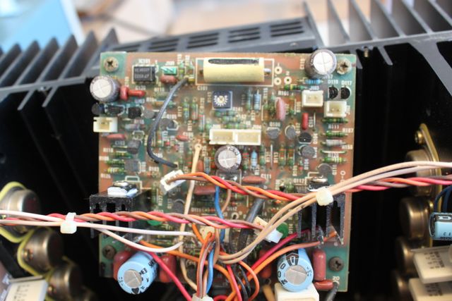
And here it is flipped over...
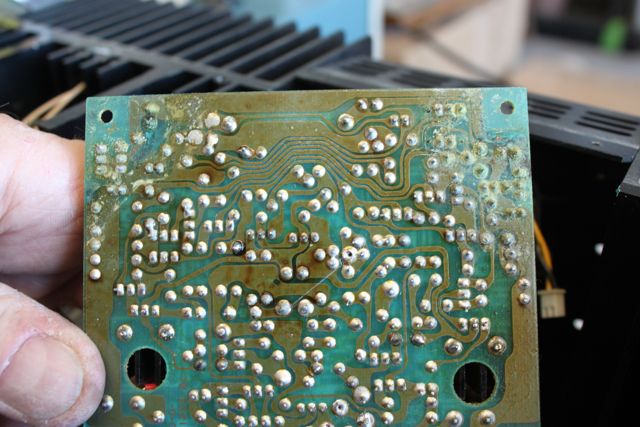
As you can see, the caps have leaked and the electrolyte has corroded the circuits in the region of the caps. This is pretty much exactly what Anatech has described. My other amp must have had the caps replaced and the board cleaned, because it was nothing like this.
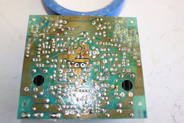
Here is a wider shot of the board too. You can see that the middle cap had also started to leak, but it had not gotten to the corrosion stage yet.
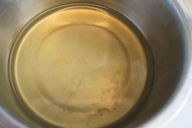
I removed the caps (what a sticky gooey mess!), and cleaned the board with my hydrocarbon cleaner (CRC carb cleaner), and most of the bad stuff came off. Here is the juice after cleaning! Remember, this stuff is clear to start...
Anatech was right, the electrolyte smells like funky burning rubber when it gets hot...
When removing the caps I had noticed that the solder joints didn't flow very well. It was almost like my iron wasn't hot enough. The solder joints that were not corroded flowed normally. So, I think the corrosion probably sucks the lead out of the solder joint, leaving a joint that is mostly Tin (which has a higher melting point). I figured this was bad, so I spent several hours carefully removing each of the components that had bad solder. . I found that the solder pads were pretty messy after removing the parts, so I used flux and solder wick to scrub them. I think the flux and the heat do some sort of number on the electrolyte, because after scrubbing with the wick and iron, there would be a black residue, that I then had to wash off with more carb cleaner.
I found that all of the parts in these affected areas had signs of corrosion on the leads. New solder would not stick to them either.. I found that, like the solder pads, applying flux and then scrubbing them with a soldering iron resulted in more black crud, that would then wash off with more cleaner..
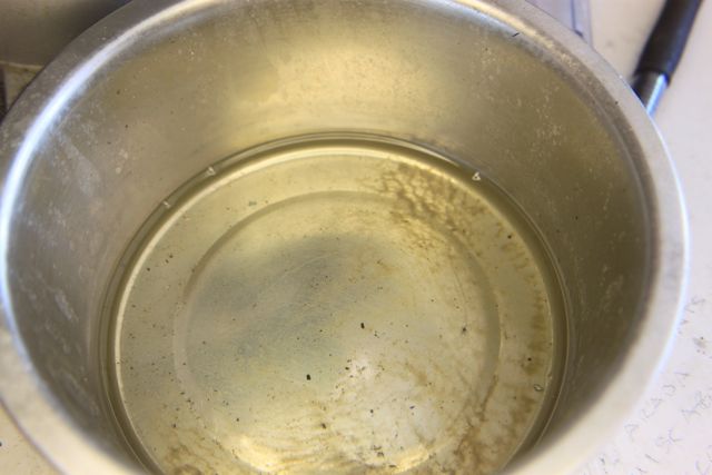
There is the catch bowl after cleaning the parts...
Once the pads and the parts were cleaned, I re-installed the parts, and then reflowed every solder joint,and cleaned the board again.
One of the zener diodes fell apart as I removed it. I guess the lead was corroded through.. You can see how funky the part is..
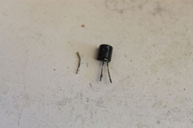
I had an LM329 left over from the other amp, so I replaced this one with that.
It is all cleaned up now, but I need one more cap, so once I get that I'll re-install the board and give it a whirl.
Cheers,
Scott
So today I finally opened it ip to have a look.
One immediately obvious observation was that, compared to my other 565, this one is in much better shape. The connections to the board for power and signal out are all done with wire-wrapped posts (my other one just had wires soldered through the holes), and it was generally very clean.
However.. I then pulled out the control board and had a look at the bottom side.. FUGLY!!!
Here is the board as found...
And here it is flipped over...
As you can see, the caps have leaked and the electrolyte has corroded the circuits in the region of the caps. This is pretty much exactly what Anatech has described. My other amp must have had the caps replaced and the board cleaned, because it was nothing like this.
Here is a wider shot of the board too. You can see that the middle cap had also started to leak, but it had not gotten to the corrosion stage yet.
I removed the caps (what a sticky gooey mess!), and cleaned the board with my hydrocarbon cleaner (CRC carb cleaner), and most of the bad stuff came off. Here is the juice after cleaning! Remember, this stuff is clear to start...
Anatech was right, the electrolyte smells like funky burning rubber when it gets hot...
When removing the caps I had noticed that the solder joints didn't flow very well. It was almost like my iron wasn't hot enough. The solder joints that were not corroded flowed normally. So, I think the corrosion probably sucks the lead out of the solder joint, leaving a joint that is mostly Tin (which has a higher melting point). I figured this was bad, so I spent several hours carefully removing each of the components that had bad solder. . I found that the solder pads were pretty messy after removing the parts, so I used flux and solder wick to scrub them. I think the flux and the heat do some sort of number on the electrolyte, because after scrubbing with the wick and iron, there would be a black residue, that I then had to wash off with more carb cleaner.
I found that all of the parts in these affected areas had signs of corrosion on the leads. New solder would not stick to them either.. I found that, like the solder pads, applying flux and then scrubbing them with a soldering iron resulted in more black crud, that would then wash off with more cleaner..
There is the catch bowl after cleaning the parts...
Once the pads and the parts were cleaned, I re-installed the parts, and then reflowed every solder joint,and cleaned the board again.
One of the zener diodes fell apart as I removed it. I guess the lead was corroded through.. You can see how funky the part is..
I had an LM329 left over from the other amp, so I replaced this one with that.
It is all cleaned up now, but I need one more cap, so once I get that I'll re-install the board and give it a whirl.
Cheers,
Scott
Last edited:
- Home
- Amplifiers
- Solid State
- Yet Another Adcom GFA-565 Thread