OK, more progress.
Since the caps were seeing 86 volts with the open zeners, I figured the op amp was toast too.
Right I was..
I replaced it, and I now have gain on the positive side of the system. The waveform at the output of the control board is distorted, probably because the negative cycle side is still inop.
I am seeing no signal gain out of Q102, so tomorrow I'll work on that..
Step by step!!
S
Last edited:
Hi Scott,
Yes, I imagine the op amp would be toast. I'm surprised that the chip hadn't split and puffed as well.
Mark all those LM329's as bad. They have been greatly abused. I would set this project aside until you have some replacement transistors and LM329's at the minimum. That op amp is a nice chip from Linear Technology noted for it's low Vos (DC offset) and low noise. What is the marking on the chip? "2A" by chance?
-Chris
The OpAmp is marked LT1010CN8.
I had a bunch of LM329s (only one left now!), so I was able to get that section of the amp working properly. No smoke, no popping caps, etc.
Both sides of that supply are now at a nice clean 14 volts.
As noted above, it looks like I have gain on the Q101/103 side, but not on the Q102/104 side. I'll check those transistors first, and see if perhaps I popped them when I messed up the pinouts.
Scott
Looks like I had a bad Q110. Replaced that and I got lots of output at pins 3 and 4 of the control board.
It turned out the distortion I was getting was because, even at its lowest stetting my function generator was putting out a little over 1 volt, which should (and did) make the amp clip. The first time I checked the output there, after fixing Q110, I had a huge square wave.. Once I put a 10:1 divider on the output of the function generator, that signal turned into a sine wave..
Hooray!!
I now need to connect up the output boards and see how that all works...and then adjust the output offset.
Whew!!
Scott
I do seem to be getting about 30 dB of gain on the control board.
Is this open loop gain? Does it go down once feedback is applied?
I ask because the control board output clips at 25 volts peak to peak at an input of only about 15 mV p-p...This corresponds to about 32 dB of voltage gain, which I recall you said was to be expected, but the input sensitivity seems very high, given that audio line voltages are about 1 volt or so.
Scott
OK, last update for a bit.
I hooked up the control board to the output sections. When I turn it on, I get about 1.4 volts DC at the output. On the scope I can see there is some oscillation, but no clear signal.
The worrying thing is that the transformer makes a loud hum, so clearly something is drawing a LOT of current. This is with no load on the output.
Hmmmm...
Scott
Looking at some older posts on this amp, this offset is often due to the OpAmp being bad.
I think I am going to try changing out the Op Amp one more time, since I am still not sure it wasn't getting some hefty voltage from the negative supply on the last go round. Have to order that, so I'll be doing real work for a few days..This time I got the LT1012A, which appears to be a slightly lower offset voltage device.
Scott
A new observation:
I decided to try disconnecting the output stages again. This time I carefully measured the signals out of the control board. BOTH point 3 and 4 (the blue and brown wire that go to the two output boards) swing from just above zero to negative 30 volts. It seems like the positive side should be swinging the other way. I was also expecting to see a waveform that was clipped at/near the zero point, but this looks like a sine wave offset by -15 volts.
These measurements are with the OpAmp removed.
I took some voltage measurements to try to determine what might be going on. Here they are:
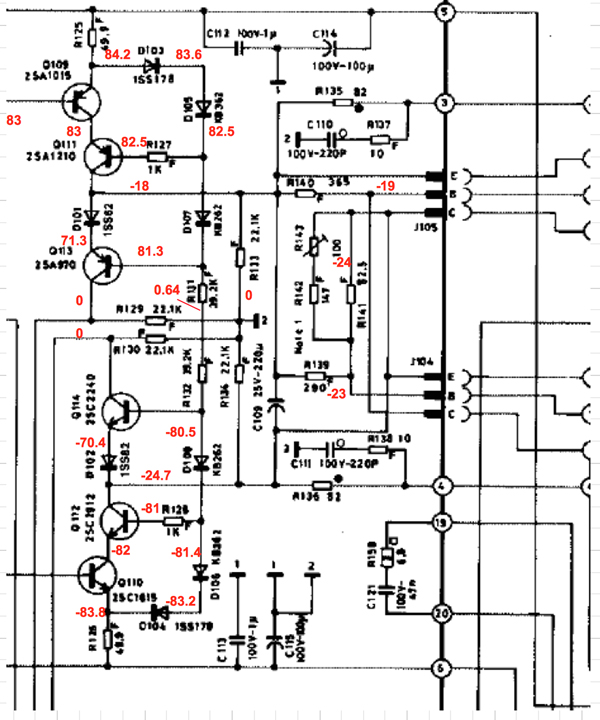
Everything seems OK EXCEPT the -18 volts at the collector of Q111. I would think this would be +20 or so. The voltage seems to be coming in via the odd network around J104 and J105, and it occurs with or without J104/105 connected. To me this implies that Q11 is either not being biased on, or it is just open.
If it were conducting then the collector would be positive, and the output would then be balanced, with something like +20 volts on one side and -20 on the other.
The alternative is that Q201 and 301 are toast, and that is messing up the bias.
Thoughts?
I decided to try disconnecting the output stages again. This time I carefully measured the signals out of the control board. BOTH point 3 and 4 (the blue and brown wire that go to the two output boards) swing from just above zero to negative 30 volts. It seems like the positive side should be swinging the other way. I was also expecting to see a waveform that was clipped at/near the zero point, but this looks like a sine wave offset by -15 volts.
These measurements are with the OpAmp removed.
I took some voltage measurements to try to determine what might be going on. Here they are:
Everything seems OK EXCEPT the -18 volts at the collector of Q111. I would think this would be +20 or so. The voltage seems to be coming in via the odd network around J104 and J105, and it occurs with or without J104/105 connected. To me this implies that Q11 is either not being biased on, or it is just open.
If it were conducting then the collector would be positive, and the output would then be balanced, with something like +20 volts on one side and -20 on the other.
The alternative is that Q201 and 301 are toast, and that is messing up the bias.
Thoughts?
Last edited:
As provided at the other thread, I had found it somewhat difficult to use the schematic in the service manual because it was separated into two pieces, and also had a bunch of fan control stuff that wasn't of any use to me (my unit doesn't have the fan assembly).
So here, for anyone's use, is the schematic from the manual joined up on a single page.
You can also view or download this at:
http://mv-makoto.com/AdcomGFA-565SchematicJoined.jpg
Hi
I am curious, in the schematic, the OPS section seems to be modular. You can put in either one pair or two pairs of pcb to get either 5 pairs output or 10 pairs output transistors.
What is the difference in the model number? Is the one with 10 pairs GFA565SE?
Last edited:
Hi Stephen,
One is a mono amplifier, so can use all positions for power output transistors. Because it is a mono amplifier, they expect it to be driven harder. Also, supply voltages are probably higher on the mono amp except for the LE model that is designed for low impedance loads.
-Chris
One is a mono amplifier, so can use all positions for power output transistors. Because it is a mono amplifier, they expect it to be driven harder. Also, supply voltages are probably higher on the mono amp except for the LE model that is designed for low impedance loads.
-Chris
Hi Scott,
I can see lots of problems. Have a look at all the emitter - base voltages. Many are in reverse breakdown. That's not very good for the transistors by the way.
Check the polarity of your transistors and make certain they are in the right places. Test for shorts while the power is off. I would recommend that you replace all the transistors that went reverse bias breakdown. Sorry about the news.
Its common that the reverse E-B breakdown will affect the beta and the noise. Those transistors are compromised now. The normal E-B breakdown occurs around 6 ~ 7 VDC whereas the forward drop will be 0.55 ~ 0.7 VDC biased forward. It depends a lot on temperature and how hard the transistor is being biased.
-Chris
I just found that the current source circuit that was working yesterday is now failed, meaning the input section is not biased at all. .
I think you are correct. All of the mashing about with backward and otherwise failed components has taken its toll on these devices.
I have some, and have ordered the rest of the semiconductors, and will replace them all. At least the caps are sound and the zeners seem to be doing their job properly..
I'll report back in a week or so.
Hi Scott,
Sorry about that discovery. I would be using a variac to slowly power these things up. You can stop if things start going south before wholesale component slaughter has occurred. Take your time on this. "If in doubt, take it out". That is cheaper than redoing the work and replacing all the other parts again.
-Chris
OK, I replaced all the transistors, and the Adcom J2 (which was open).
I had -40 volts on the collectors of Q111 and Q112, and the thing still dimmed the lights and hummed loudly when I connected the control board to the output stages.
All of the other voltages looked OK (transistors biased in the right direction), so I decided to look at the only transistors I didn't change. These are the ones mounted to the output heatsinks.
I found that the SA1376 transistor mounted on the output heatsink was bad. Man was that a pain to replace!!
I have not yet replaced the other one. I now have about 16 volts on the collector of Q111, and 11 volts on the collector of Q112 (See below).
I would assume that the collectors of these should be about the same but opposite in polarity, so obviously something is still wrong, but not as wrong as it was before..
Tomorrow I'll swap out the other heatsink transistor, and see how that works. I think I'll also check the pot (R143) since it seems to have zero impact on any of the biasing.
Do you know what the collectors should be at?
I have plenty of gain now, but I think the biasing is still off at the control board output. What should those signals look like?
I would think they would be sine waves offset by some amount to create the proper biasing for the AB output stage.
Scott
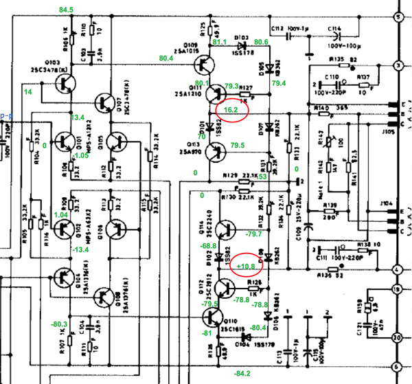
OK, I have been all over this thing. I discovered that D102 was shorted (not SHORTED, but it had 0.1 volts offset in either direction).
I have gain through both sides of the input stage (Q111 and Q112)..
BUT...
I cannot seem to get the DC offsets at the collectors of Q111 and Q112 to behave.
I get about -57 volts at each of the collectors.
I removed C109 and disconnected R139, which is the path between these two sides, and I get +/-80 odd volts on each respectively. So they seem to be behaving properly on their own. The issue is either something in the weird bias network involving Q201 and Q301, or it is some current imbalance which makes the negative side dominate when they are connected together through that bias network.
I am about to toss this thing in the trash...
S
A long technical post....
I went and took some very careful measurements of the system with R139 and C109 removed. This separates the negative and positive signal sides, so I can see how they behave independently. Operating separately, I get about +/-82 volts on the respective collectors of Q111 and Q112. However, I also looked at an audio signal on these stages using my scope. My scope isn't particularly good (I just bought a new one on eBay, so that will be helpful when it arrives), but I was able to get a feel for the signals on each side from this.
The service manual states that the gain stages are "class A". However, this seems to be not quite correct. Obviously the input stages are full Class A. The outputs of each side of the input gain stage circuit swing over the full signal cycle, but it seems like the "driver stage (the one that drives the output stage) needs to be Class AB (maybe they mean the combined set of positive and negative circuits is class A.. Not sure I'd call it that...)
Based on the way the mid gain stage (Q109/Q111) is connected to the output gain stage the mid gain stage should do one of the following:
1) Swing between 0 and full scale (about 75 volts) for the positive or negative half cycle (plus a little bit to make it class AB vs class B). This would be a true AB drive stage for the output stage.
2) Swing between 0 and 75 volts over the full signal period on one side, and between 0 and -75 volts over the full signal period for the other side
If the second of these is the case, then the input stage of the output would be in cutoff over half of the signal period. The problem with this is that the signal would only go between 37.5 and 75 volts on one side and between -37.5 v and -75 volts on the other. So there is a large missing region between -37.5 and +37.5.
A third possibility is that each mid stage swings between +75 and -75 volts. The problem with this is that the topology doesn’t seem to allow for this, since each collector load resistor is grounded.
So it seems like option 1 is the most reasonable. This sort of seems to be what I am seeing on the scope, when the gain blocks are operated separately (i.e. with R139 disconnected, so there is no bias offset between the positive and negative sections of the circuit). I get a sort of half cycle looking waveform.
The question then is why does the negative side overwhelm the positive side?
I think the issue is that the negative side is biased into saturation all the time, so basically only when the input signal pushes the operating point up into the linear region for the device do we start to see the signal at the load resistor fall. I see this in the wave form too, which seems to only get the peak of the signal, so it is basically biased on with no signal applied, and only biased off at the peak of the applied signal (remember, in this circuit the emitter is connected through a resistor to the rail, so lower voltage input at the base means higher current, and a higher voltage on the load resistor (which is connected to ground).
So this appears to be either a stage bias problem (which doesn’t seem right, since the bias there is set by the diode chains (e.g D 103-107), and this seems pretty much the same for both sides), or the input signal (in this case the negative side input signal) is offset too far positive (or not negative enough), causing the driver stage to saturate. When that stage is saturated, then the load resistor will see -82 volts, and the system will deliver enough current to bleed through the output bias network to drive the positive side negative.
So, this seems to be primarily an issue with the offset from the negative side input stage being too low (insufficiently negative).
Looking at the diagram below, it is clear that if the base voltage at the input is too low, then the driver transistor will be biased too high, and VCE will be too low, even with no applied signal.
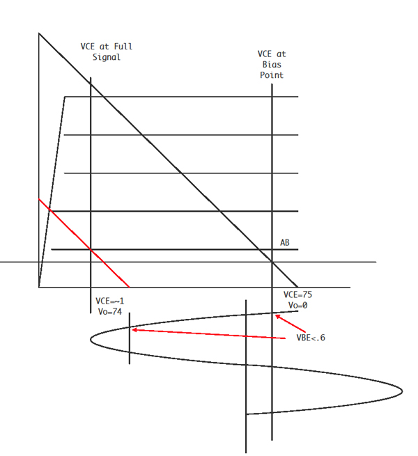
For this to occur, the current at the input stage would need to be too high, causing the drop across the input load (R106/107) to be too high, thereby lowering the voltage at the base of the driver (Q109/110)/
The input stage biases are:
Positive side: 40 mV across 32.2 ohms, or 1.2 mA
Negative side: 50 mV across 32.2 Ohms, or 1.6 mA
Clearly the negative side is higher! 33% higher…
Looking back over this saga, I found that at some point one of the LEDs on the board was dead. I am not sure if it was always dead, or died during troubleshooting. I didn't have a direct replacement, but used a different LED that I had (one that I used when matching the Darlingtons). I suspect that the device has a slightly higher Vf, and this biases the current source for the negative side differential pair at the higher current level. At 1.2 mA, the 1 K load resistor (R106) will drop 1.2 volts. At 1.6 mA the other 1K load resistor (R107) will drop 1.6 volts. Since VBE on the drivers will be the same (assume 0.6 volts), then the base voltage on Q110 will be 85-1.6=83.4v. So the emitter will be 84 volts (83.4+.6). One volt dropped across R126 (which is 49.9 ohms) is 20 mA.
In contrast, the same analysis applied to the positive side (Q111) comes up with: 1.2 V dropped across the 1K load resistor means that the base voltage on Q111 will be 85-1.2=83.8v. So the emitter will be 84.4 volts (83.8+.6). 0.6 volts dropped across R125 (which is 49.9 ohms) is 12 mA.
So the negative side is running 8 Ma more.. Which is 66% higher.. No wonder the output is unbalanced!!
The other corroborating evidence for this is that the waveform on the negative side is goes from about -75 to -70 volts and only covers about 10-15% of the cycle, whereas the waveform on the positive side (with the two sides separated as described above) goes from about 0 to 75 volts and covers at least 1/2 the cycle...
Once my new scope arrives, I'll take some photos..
I must say, that, despite the frustrations with this beast, I have dusted off a lot of circuit theory from 40 years ago..
It is also interesting to note that, while I measured the voltages at various points in the circuit, the higher rail voltages tend to drift around a bit, so it is very difficult to tell that one leg is a few tenths of a volt higher than another. In contrast, the low voltages at the diff pairs are very stable, and it is easy to see a few mV difference.. those small differences get multiplied up in the gain stages and can create big trouble, as we have seen!!
Cheers,
Scott
I went and took some very careful measurements of the system with R139 and C109 removed. This separates the negative and positive signal sides, so I can see how they behave independently. Operating separately, I get about +/-82 volts on the respective collectors of Q111 and Q112. However, I also looked at an audio signal on these stages using my scope. My scope isn't particularly good (I just bought a new one on eBay, so that will be helpful when it arrives), but I was able to get a feel for the signals on each side from this.
The service manual states that the gain stages are "class A". However, this seems to be not quite correct. Obviously the input stages are full Class A. The outputs of each side of the input gain stage circuit swing over the full signal cycle, but it seems like the "driver stage (the one that drives the output stage) needs to be Class AB (maybe they mean the combined set of positive and negative circuits is class A.. Not sure I'd call it that...)
Based on the way the mid gain stage (Q109/Q111) is connected to the output gain stage the mid gain stage should do one of the following:
1) Swing between 0 and full scale (about 75 volts) for the positive or negative half cycle (plus a little bit to make it class AB vs class B). This would be a true AB drive stage for the output stage.
2) Swing between 0 and 75 volts over the full signal period on one side, and between 0 and -75 volts over the full signal period for the other side
If the second of these is the case, then the input stage of the output would be in cutoff over half of the signal period. The problem with this is that the signal would only go between 37.5 and 75 volts on one side and between -37.5 v and -75 volts on the other. So there is a large missing region between -37.5 and +37.5.
A third possibility is that each mid stage swings between +75 and -75 volts. The problem with this is that the topology doesn’t seem to allow for this, since each collector load resistor is grounded.
So it seems like option 1 is the most reasonable. This sort of seems to be what I am seeing on the scope, when the gain blocks are operated separately (i.e. with R139 disconnected, so there is no bias offset between the positive and negative sections of the circuit). I get a sort of half cycle looking waveform.
The question then is why does the negative side overwhelm the positive side?
I think the issue is that the negative side is biased into saturation all the time, so basically only when the input signal pushes the operating point up into the linear region for the device do we start to see the signal at the load resistor fall. I see this in the wave form too, which seems to only get the peak of the signal, so it is basically biased on with no signal applied, and only biased off at the peak of the applied signal (remember, in this circuit the emitter is connected through a resistor to the rail, so lower voltage input at the base means higher current, and a higher voltage on the load resistor (which is connected to ground).
So this appears to be either a stage bias problem (which doesn’t seem right, since the bias there is set by the diode chains (e.g D 103-107), and this seems pretty much the same for both sides), or the input signal (in this case the negative side input signal) is offset too far positive (or not negative enough), causing the driver stage to saturate. When that stage is saturated, then the load resistor will see -82 volts, and the system will deliver enough current to bleed through the output bias network to drive the positive side negative.
So, this seems to be primarily an issue with the offset from the negative side input stage being too low (insufficiently negative).
Looking at the diagram below, it is clear that if the base voltage at the input is too low, then the driver transistor will be biased too high, and VCE will be too low, even with no applied signal.
For this to occur, the current at the input stage would need to be too high, causing the drop across the input load (R106/107) to be too high, thereby lowering the voltage at the base of the driver (Q109/110)/
The input stage biases are:
Positive side: 40 mV across 32.2 ohms, or 1.2 mA
Negative side: 50 mV across 32.2 Ohms, or 1.6 mA
Clearly the negative side is higher! 33% higher…
Looking back over this saga, I found that at some point one of the LEDs on the board was dead. I am not sure if it was always dead, or died during troubleshooting. I didn't have a direct replacement, but used a different LED that I had (one that I used when matching the Darlingtons). I suspect that the device has a slightly higher Vf, and this biases the current source for the negative side differential pair at the higher current level. At 1.2 mA, the 1 K load resistor (R106) will drop 1.2 volts. At 1.6 mA the other 1K load resistor (R107) will drop 1.6 volts. Since VBE on the drivers will be the same (assume 0.6 volts), then the base voltage on Q110 will be 85-1.6=83.4v. So the emitter will be 84 volts (83.4+.6). One volt dropped across R126 (which is 49.9 ohms) is 20 mA.
In contrast, the same analysis applied to the positive side (Q111) comes up with: 1.2 V dropped across the 1K load resistor means that the base voltage on Q111 will be 85-1.2=83.8v. So the emitter will be 84.4 volts (83.8+.6). 0.6 volts dropped across R125 (which is 49.9 ohms) is 12 mA.
So the negative side is running 8 Ma more.. Which is 66% higher.. No wonder the output is unbalanced!!
The other corroborating evidence for this is that the waveform on the negative side is goes from about -75 to -70 volts and only covers about 10-15% of the cycle, whereas the waveform on the positive side (with the two sides separated as described above) goes from about 0 to 75 volts and covers at least 1/2 the cycle...
Once my new scope arrives, I'll take some photos..
I must say, that, despite the frustrations with this beast, I have dusted off a lot of circuit theory from 40 years ago..
It is also interesting to note that, while I measured the voltages at various points in the circuit, the higher rail voltages tend to drift around a bit, so it is very difficult to tell that one leg is a few tenths of a volt higher than another. In contrast, the low voltages at the diff pairs are very stable, and it is easy to see a few mV difference.. those small differences get multiplied up in the gain stages and can create big trouble, as we have seen!!
Cheers,
Scott
Last edited:
So I spent some quality time really understanding the Diff pair bias current circuit.
This circuit turns out to be key to the overall performance of this amplifier. If the tail currents are not set up correctly, then the bias current in the two diff pairs (positive side and negative side) will be different, and this will make the drop across the 1K Ohm front section load resistors (R106 and R107) slightly different.
For example, the drive current is supposed to be about 3 mA for the pair, or 1.5 mA for each leg. That would produce a drop of about 1.5 volts at the load resistor. If the currents are mismatched by, say .1 mA, then the load resistor voltages will be off by about 0.1 volts...
Now, this might not seem like much, but the gain of the following stage is about 200..so this offset will get multiplied by a factor of 200, and because the amplifier is DC coupled, that offset will propagate through the gain stage resulting in an output offset of 20 volts!!!
Normally when these are balanced, the voltages in the bias circuit formed by Q201 and Q301 (those odd transistors off on the output boards that are embedded in the heatsinks) are balanced. This means that the voltage at R139 (the balance point in the diagram below) should be about zero...
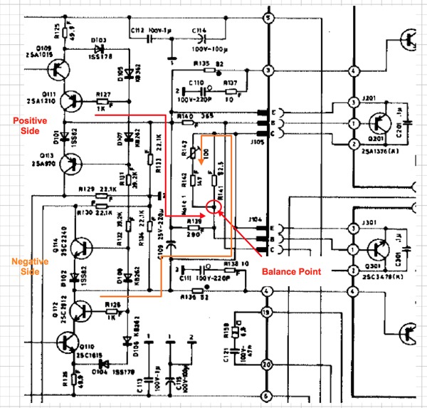
The servo can adjust some of this out, but the worse the offset, the more it has to do. Essentially what happens is that the Q111/Q112 stages start fighting each other. Whichever one has the higher bias offset will conduct more current, and once the servo runs out of steam (the op AMP output rails), the circuit can't compensate, and the DC offset at the output rises. In my amp, this offset meant that the offset at the balance point was about -55 volts (because the negative side diff pair was biased on higher than the positive side.
In practice, when the offset is large enough, it can drive the collector of Q111 (or Q112 - depending on which side of the diff pairs is biased more) to a high value in the wrong direction.
So bottom line is that the core driver of offset problems in these amplifiers is the diff pair bias circuit formed by Q115 to Q118.
Below is an example of how it is supposed to operate.
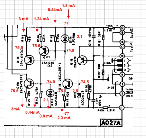
Here you can see that everything is in balance. The core issue here is that the LEDs (D113 and D114) must be the same, and they must have a voltage drop that corresponds to the voltage of the zener diode regulator D115 (The Adcom J6 part).
However, if the LED are different, OR if the voltage drop across them is not the proper ratio relative to the drop at D115, then all hell breaks loose!!!
I have not analyzed yet how the relationship between the value of D115 and the LED drops works, but here is an example of how mine changed with the wrong LEDs. Remember it was operating oddly when the LEDs were unequal, and it got even weirder when I made them both the same, but the wrong voltage drop value (in this case 1.6 volts instead of the 2.1 volt value as designed), so this circuit can go wrong in two different ways. An example of the matched but incorrect LED drops is shown below.
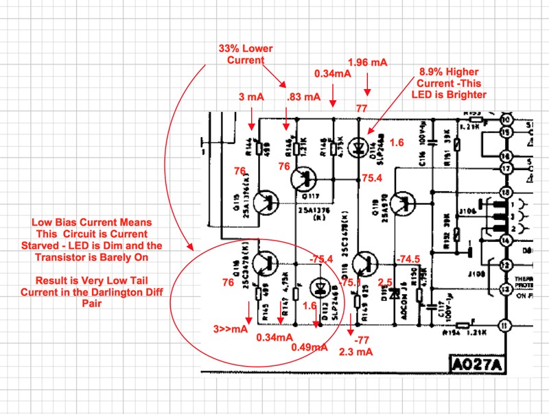
Here you can see that the lower LED drop combined with the unchanged value at D115 means that Q117 passes less current. Even though the voltage at the base of Q116 is the same as that at Q115, the current through Q117 is 33% lower than it is supposed to be (See diagram above).
The visible upshot of this was that the LED was barely glowing.. The circuit upshot was that the current in the positive side Diff pair was about 0.2 mA, making the drop across R106 too low, and thus causing Q111 to conduct less current than Q112...
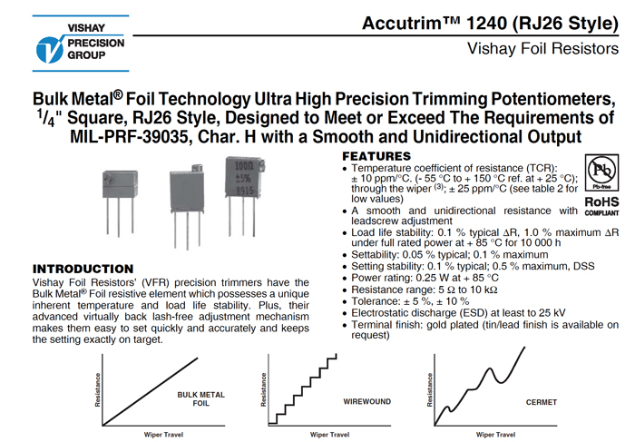
Having done all of this, I am of the opinion that R144 and 145 (the resistors that set these current values) should actually be adjustable, so that you can tune the resulting tail currents fairly precisely. That way the balance can be tuned up front, and the servo and R143 in the output bias circuit can compensate for any minor thermal variations.
Once I get the amp basically working, I'll explore this option. I found a very high quality foil trim pot made by Vishay. It is a multi turn device with a super smooth and well controlled resistance vs position characteristic. The down side to this is that they are $13 each, which explains why Adcom didn't use this approach.
Cheers!
Scott
This circuit turns out to be key to the overall performance of this amplifier. If the tail currents are not set up correctly, then the bias current in the two diff pairs (positive side and negative side) will be different, and this will make the drop across the 1K Ohm front section load resistors (R106 and R107) slightly different.
For example, the drive current is supposed to be about 3 mA for the pair, or 1.5 mA for each leg. That would produce a drop of about 1.5 volts at the load resistor. If the currents are mismatched by, say .1 mA, then the load resistor voltages will be off by about 0.1 volts...
Now, this might not seem like much, but the gain of the following stage is about 200..so this offset will get multiplied by a factor of 200, and because the amplifier is DC coupled, that offset will propagate through the gain stage resulting in an output offset of 20 volts!!!
Normally when these are balanced, the voltages in the bias circuit formed by Q201 and Q301 (those odd transistors off on the output boards that are embedded in the heatsinks) are balanced. This means that the voltage at R139 (the balance point in the diagram below) should be about zero...
The servo can adjust some of this out, but the worse the offset, the more it has to do. Essentially what happens is that the Q111/Q112 stages start fighting each other. Whichever one has the higher bias offset will conduct more current, and once the servo runs out of steam (the op AMP output rails), the circuit can't compensate, and the DC offset at the output rises. In my amp, this offset meant that the offset at the balance point was about -55 volts (because the negative side diff pair was biased on higher than the positive side.
In practice, when the offset is large enough, it can drive the collector of Q111 (or Q112 - depending on which side of the diff pairs is biased more) to a high value in the wrong direction.
So bottom line is that the core driver of offset problems in these amplifiers is the diff pair bias circuit formed by Q115 to Q118.
Below is an example of how it is supposed to operate.
Here you can see that everything is in balance. The core issue here is that the LEDs (D113 and D114) must be the same, and they must have a voltage drop that corresponds to the voltage of the zener diode regulator D115 (The Adcom J6 part).
However, if the LED are different, OR if the voltage drop across them is not the proper ratio relative to the drop at D115, then all hell breaks loose!!!
I have not analyzed yet how the relationship between the value of D115 and the LED drops works, but here is an example of how mine changed with the wrong LEDs. Remember it was operating oddly when the LEDs were unequal, and it got even weirder when I made them both the same, but the wrong voltage drop value (in this case 1.6 volts instead of the 2.1 volt value as designed), so this circuit can go wrong in two different ways. An example of the matched but incorrect LED drops is shown below.
Here you can see that the lower LED drop combined with the unchanged value at D115 means that Q117 passes less current. Even though the voltage at the base of Q116 is the same as that at Q115, the current through Q117 is 33% lower than it is supposed to be (See diagram above).
The visible upshot of this was that the LED was barely glowing.. The circuit upshot was that the current in the positive side Diff pair was about 0.2 mA, making the drop across R106 too low, and thus causing Q111 to conduct less current than Q112...
Having done all of this, I am of the opinion that R144 and 145 (the resistors that set these current values) should actually be adjustable, so that you can tune the resulting tail currents fairly precisely. That way the balance can be tuned up front, and the servo and R143 in the output bias circuit can compensate for any minor thermal variations.
Once I get the amp basically working, I'll explore this option. I found a very high quality foil trim pot made by Vishay. It is a multi turn device with a super smooth and well controlled resistance vs position characteristic. The down side to this is that they are $13 each, which explains why Adcom didn't use this approach.
Cheers!
Scott
Last edited:
If you folks refer back to the start of this thread, you may recall that the previous owner had put in some trim pot networks at R106 and R107 (the 1K load resistors on the diff pairs).
I think this was an attempt to manage the DC offset. The problem with this approach is twofold. For starters, it is curing the symptom (DC offset voltage at the Q111/Q112 inputs), and not the root cause (DC Current offset between the positive and negative Diff pairs).
More importantly, by changing the load resistors he was changing the gain (remember, in this amplifier, once past the big yellow input blocking cap, gain goes all the way to DC..), and so while you might be able to adjust the DC offset this way, you would also cause the gain to be different for one side vs the other of the AB push/pull arrangement. That would essentially introduce some form of distortion, wherein the positive half cycle of the audio signal would be different from the negative half cycle...
Glad I ditched that "fix"..
By varying the R144/R145 resistors you can adjust the bias currents, and thus the DC level at the inputs to Q111 and Q112, without significantly impacting the circuit gains.
Here is what I plan to use. As noted above, the only problem with these is the cost. Depending on the package and the resistance value, they range from $12 to $40...each....
Hi Scott,
You know they made a ton of these with normal production tolerances, and none suffered this kind of issue that I know of. You can always check the health of the circuit by looking at the output of the servo amp.
As you have noticed, the LEDs serve as a reference voltage for the CCS circuits. You could use a voltage reference IC to replace the LEDs if it was really a problem, but the adjustment range of the servo is vast. I will say that I'm not a fan of a circuit that isn't naturally balanced and only needs a nudge from a servo..
-Chris
Yeah, that's why I am going to wait and see if I need to do something like that to balance things. Having looked this over a bot more, I suspect it is not that sensitive..
I went through the circuit and figured out what voltages I should be seeing where, and then traced the entire board.
I found several things:
As you recall the PO had done some oddball things with the various diodes. I had replaced the KB262 and KB362 diodes, since they were obviously jury rigged. However, this time, when I went to check the D103/D104 pair (the ones at the top ends of the bias diode stack), I found that they only had a forward voltage of about 0.5 volts. The data sheet says they should have a forward voltage of about 1.1, so these diodes had biased the Q109/Q110 pair slightly incorrectly (a little too low).
Once I fixed that, I still had -57 volts on both outputs.
After a lot of sleuthing, involving isolating various parts of the circuit, I found that D102 and Q114 were both shorted. These are in the clipping sensing circuit. Once I changed those out, I got a reasonably balanced output where the drive lines to the output stage are at about 2 volts or so..which seems about right. It may not be perfect, but it is clearly operating more as it is supposed to.
I hooked up the output stages, and the feedback line, and tried it out. The drive lines do not react badly to this, and nothing smokes.. so that's a start...
So, it seems that the control board is FINALLY straightened out...
HOWEVER, when the output stages are connected, the transformer makes a loud buzzing/hum sound, which tells me that something is drawing a lot of current in the output stage. I suspect I have an issue with a shorted output transistor or something.
It is interesting to note that there is no hum when I disconnect the output lines (the wires connected to terminals 3 and 4 on the control board), so whatever is happening seems to be related to the input bias.
Any ideas on how to approach this?
What should the voltages levels on the input lines to the output stage be (terminals 3 and 4 on the control board)???
Thanks for your help so far on this! It feels good to make some progress..
Scott
- Home
- Amplifiers
- Solid State
- Yet Another Adcom GFA-565 Thread