With the LT1818, did you have to change any other parts for stability. Can you also describe other changes?
There is no need to change anything for stability..
I said already, only two things changed, opamps and output capacitors..
Attachments
Last edited:
Did someone tested what is playing better, sharp or slow roll-off filter..
At first it seemed to me that there is no difference, so I left sharp.. yesterday I changed filters few times and listened more carefully.. now it seems that there are small differences, slow plays better..
At first it seemed to me that there is no difference, so I left sharp.. yesterday I changed filters few times and listened more carefully.. now it seems that there are small differences, slow plays better..
Could this XMOS interface be used as USB receiver for a Buffalo IIISE ES9018 DAC (connecting to I2s/DSD inputs on the DAC board)?
If it could, what adjustments should be done to pin configurations/shorting or other? And what should be the connection pins used?
I think this should be better performing than an Amanero board, isn't it?
If it could, what adjustments should be done to pin configurations/shorting or other? And what should be the connection pins used?
I think this should be better performing than an Amanero board, isn't it?
Could this XMOS interface be used as USB receiver for a Buffalo IIISE ES9018 DAC (connecting to I2s/DSD inputs on the DAC board)?
If it could, what adjustments should be done to pin configurations/shorting or other? And what should be the connection pins used?
I think this should be better performing than an Amanero board, isn't it?
I am using this interface with my Buffalo III SE. The only adjustment for using the ES9018 DAC chip is to place a 47k resistor between pins 1 & 5 as noted in the manual.
I also purchased two of the JLSounds power supplies to power each side (USB & reclocking) of the board in order to take advantage of the galvanic isolation.
Strange... i can't find that information in the manual i see in jlsounds site... maybe the manual version on the site is an old one?
The manual is at: http://jlsounds.com/uploads/Specifications.pdf
Thanks, now i can find that statement in table 1, so it's clear to me i have to connect pin 1 to pin 5 through 4,7 kO resistance.
But what's table 2 about?
I did not do anything with regards to Table 2. Only Table 1.But what's table 2 about?
I did not do anything with regards to Table 2. Only Table 1.
Thanks again! 😉
Hi Joro,
Did you finally planed the possibility to launch your board with an option for the simultanous mode for the TDA1541 ?
Do you plan with you excellent actual board for some better output layout for the gnd outputs : not only one pin 11 Gnd but one gnd pin near each I2S output pin to allow each I2S signal to have a closest and individual return path= less jitter, better shielving & EMC like uf.l connector allows ?
My understanding after some exchange with JLsounds is you have just a trace on the actual pcb for an uf.l conector for the MCLK signal !
Thanks for your answer about that, I'm sure some could appreciate this little modification for the actual board as some others could consider the board if exist for the TDA1541A as your board is well priced.
regards
Pin 8
What is the purpose of Pin 8?
I am able to play (at least I think I am) DSD files using DoP so I am not sure what Pin 8 is doing with regards to the 3.3V for DSD.
Currently, I do not have anything connected to Pin8 for my Buffalo IIISE DAC (ES9018).
Could someone (Joro) please let me know about this?
Hi,
Only DSD64 over S/PDIF is possible with a little modification of the firmware
Current firmware should be almost rewritten to have simultaneous mode for the TDA1541, this was the reason that I haven’t written the firmware for this mode and that’s why it’s not announced 🙂 If there are enough people who want it, there is no problem to make a small external PCB board (this will significantly faster) with a CPLD. But one have to make additional reclock, because the CPLD would bring contribution for the jitter 🙂 The only complication is to find some spare time, which this summer is a deficit 🙁.
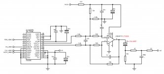
I attached a picture of the new oscillator daughter board. There is no option for TI regulator, because according to the tests wasn’t as good as ADM7150. On this board there is uf.l connector, but if one wants to use it, have to solder and a buffer (there is a place for the buffer on the oscillator board).
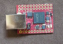
As for advanced diyers, I’ve designed OEM module, based on XMOS U series. As one can see from the attached picture the board is “naked” – without isolation, reclock and oscillators, this would give much more flexibility during the realization of the diyers projects and on this board next to every I2S signal line there is a GND
Actually this is the answer to
ES9018 automatically detects the DSD signal and that’s why it doesn’t need to use pin8. Almost all the rest DACs, which can play DSD, need an additional software control for their internal registers for DSD/PCM changing. Then this signal is used from a microcontroller, which controls the used DAC.
I attached you a scheme for full indication 🙂
Regards,
Joro
Any chance to support DoP DSD128 over SPDIF? Understand the limitation of transformer, while hopefully there is alternative way using other isolation .
Only DSD64 over S/PDIF is possible with a little modification of the firmware
Did you finally planed the possibility to launch your board with an option for the simultanous mode for the TDA1541 ?
Current firmware should be almost rewritten to have simultaneous mode for the TDA1541, this was the reason that I haven’t written the firmware for this mode and that’s why it’s not announced 🙂 If there are enough people who want it, there is no problem to make a small external PCB board (this will significantly faster) with a CPLD. But one have to make additional reclock, because the CPLD would bring contribution for the jitter 🙂 The only complication is to find some spare time, which this summer is a deficit 🙁.
Do you plan with you excellent actual board for some better output layout for the gnd outputs
I attached a picture of the new oscillator daughter board. There is no option for TI regulator, because according to the tests wasn’t as good as ADM7150. On this board there is uf.l connector, but if one wants to use it, have to solder and a buffer (there is a place for the buffer on the oscillator board).
As for advanced diyers, I’ve designed OEM module, based on XMOS U series. As one can see from the attached picture the board is “naked” – without isolation, reclock and oscillators, this would give much more flexibility during the realization of the diyers projects and on this board next to every I2S signal line there is a GND
Actually this is the answer to
Are you planning some new toys for us?
What is the purpose of Pin 8?
I am able to play (at least I think I am) DSD files using DoP so I am not sure what Pin 8 is doing with regards to the 3.3V for DSD.
Currently, I do not have anything connected to Pin8 for my Buffalo IIISE DAC (ES9018).
ES9018 automatically detects the DSD signal and that’s why it doesn’t need to use pin8. Almost all the rest DACs, which can play DSD, need an additional software control for their internal registers for DSD/PCM changing. Then this signal is used from a microcontroller, which controls the used DAC.
I attached you a scheme for full indication 🙂
Regards,
Joro
Attachments

Last edited:
Hi Joro,
Nice to see you active on this thread again. I'm also quite happy to see a pic of the oscillator daughter board as I'm very much interested in it.
When will this product be ready? Also, can you show how it will connect to the main board? (In my case, an I2SoverUSB with AK4396)
Nice to see you active on this thread again. I'm also quite happy to see a pic of the oscillator daughter board as I'm very much interested in it.
When will this product be ready? Also, can you show how it will connect to the main board? (In my case, an I2SoverUSB with AK4396)
Hi,
Only DSD64 over S/PDIF is possible with a little modification of the firmware
Current firmware should be almost rewritten to have simultaneous mode for the TDA1541, this was the reason that I haven’t written the firmware for this mode and that’s why it’s not announced 🙂 If there are enough people who want it, there is no problem to make a small external PCB board (this will significantly faster) with a CPLD. But one have to make additional reclock, because the CPLD would bring contribution for the jitter 🙂 The only complication is to find some spare time, which this summer is a deficit 🙁.
I attached a picture of the new oscillator daughter board. There is no option for TI regulator, because according to the tests wasn’t as good as ADM7150. On this board there is uf.l connector, but if one wants to use it, have to solder and a buffer (there is a place for the buffer on the oscillator board).
As for advanced diyers, I’ve designed OEM module, based on XMOS U series. As one can see from the attached picture the board is “naked” – without isolation, reclock and oscillators, this would give much more flexibility during the realization of the diyers projects and on this board next to every I2S signal line there is a GND
Regards,
Joro
Hi Joro,
Thank you for your answers.
Sounds of the Nature during the summer and time/rest for oneself & family can not be swapped 🙂
I don't know but for myself about the real need of a board for the TDA1541but I surmise some could be interrested if the layout & pricing please them. I suggest here to ask in two threads I opened for beginners like me about the Distinction-1541 coreboards (which have both uf.l I2S inputs connectors as VIAS in a SGSGSGSG -Simultanous mode possible- layout for its input data signals. May you agree I ask them and link to this thread for showing their interrest by asking boards (interrest grup buy) ?
It could give you pragmatic to see if it's enough to continue or not on the TDA1541 path ! I believe a pricing of the boards could allow them to decide more easily.
Wow.... the clock board and oem XMos photographs look great. My understanding is the clock board is maid for the OEM module : am I right ?
Do they allow simultanous mode or the advanced diyer has to programm the Xmos ?
If there is a plan to stack the clock board and the actual JLSounds simultanous USBoverPCM clock board (simultanous mode for AD186x & PCM dac chip family) how is solved the I2S layout output connection to the clock board ? (how are they connected together ? Any photograph ?)
According to me the good actual board seems good enough but this problem of gnd layout to connect it with most dac boards who have GndSignalGSGS I2S connector and not just GSSS as the actual JLSounds board, also because RF signal works better with a close signal return path for each RF signal... btw this is my understandings as a beginner when reading some entries on Diyaudio 😱)
Thanks again Joro for those nice exchanges with you and JLSounds, let me know about the links here if wanted.
Regards
Eldam
Last edited:
I just checked Joro's site (jlsounds.com) and found that the oscillator board is already listed there as for sale!
I'm not entirely sure though as to how it should connect to the main board. Should it be stacked over or under? Also, how will the over all solution be powered? If I put in a separate supply for the AK4396 and the oscillator board, do I still need to power the main board?
Hope that Joro can answer these questions 🙂
I just checked Joro's site (jlsounds.com) and found that the oscillator board is already listed there as for sale!
I'm not entirely sure though as to how it should connect to the main board. Should it be stacked over or under? Also, how will the over all solution be powered? If I put in a separate supply for the AK4396 and the oscillator board, do I still need to power the main board?
Hope that Joro can answer these questions 🙂
Ok... Thanks for the infor... I think i will just hit the add to cart button and find out 🙂
edit... at the product page... there is a more infor button where it tell most of the things...
http://jlsounds.com/uploads/Oscil.pdf
Last edited:
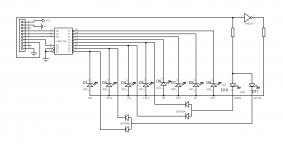
Look at the photograph with the little uf.l connector board stacked on the Joro I2StoPCM board : exactly what I need if JLSounds don't want to increase the quality of the output layout with GSGSGSG grounding arrengement : NOS 384 AD1865 with built in LDR : it don't resolve the unique output gnd pin of the board but help to provide bigger length with coax uf.l wires....
Anybody knows where this little board can be sourced ? A diyer work ?
Anybody knows where this little board can be sourced ? A diyer work ?
- Home
- Source & Line
- Digital Line Level
- XMOS DSD 384 kHz / 32bit USB