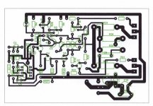
I do not think we used same schematic but we have both used same fantastic idea, namely the Mooly Amp for music. So we should end up with exactly same board. Unless one of us (me) have done something really wrong. I can't just spot where I have done wrong. Warning I am a noob,
Do any of you please take a look and hopefully point out where my pcb is wrong?
I have tried to redraw the entire pcb, three times but do arrive at the same error, every time.
Do any of you please take a look and hopefully point out where my pcb is wrong?
I have tried to redraw the entire pcb, three times but do arrive at the same error, every time.
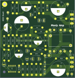
I'm not sure the middle picture layout would be successful tbh because apart from any 'known error/s' it seems to have a huge amount of copper land that is actually the output signal (assuming I am looking at it correctly? am I? ) and also the drivers are very remote from the output transistors (they need to be quite close) with the gate resistors need to be right up to the gate lead on the FET's.
Thanks, I'll try to investigate and report back🙂
EDIT:
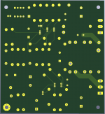
This is how the board looks like without any of the "copper filled zones"
I am not sure what you mean about the components, having to be near each other, would you please write the component numbers you are talking about? 🙂
i.e Q5, R17 shall be near L1
EDIT:
This is how the board looks like without any of the "copper filled zones"
I am not sure what you mean about the components, having to be near each other, would you please write the component numbers you are talking about? 🙂
i.e Q5, R17 shall be near L1
Attachments

Last edited:
OK 🙂
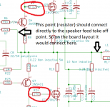
Just have a look at this (untested and probably not finalised) single sided layout I did from years ago. It doesn't look pretty but look at the FET gate resistors and also look at the critical feedback take off point which is directly on the 0.22 ohm series output resistor node. That physical point (the junction of the feedback resistor and the actual output) is extremely important because that takeoff point is where the feedback has correctly applied itself.
Does that make sense? You can move the feedback point around but the series 0.22 ohm should also follow it.
The layout is the view of the copper looking down and through the board... which is how you do it if you produce a transparency to etch your own.
And the coil isn't shown either.
Attachments
It not easy following images tbh, they make sense to you because you are working with it all time from different angles.
The things I mentioned about the feedback point and the gate resistors are pretty important. You need those resistors up close to the FET gate. Also its not a good idea to have lots of copper pour (the big areas of copper) that are signal carrying areas. Grounds and supplies are fine to do that with but not signal because then it will just radiate that signal all around which we don't want.
I know its not easy 🙂 and your doing really well for a first attempt at a board.
Yes I know it's almost imposible to follow, but there have to be a way to show it all, hmm maybe the desifn part of KiCad is useable.
Am I right in thinking you are talking about the R9 and R19 or/and R5 and R24?
Am I right in thinking you are talking about the R9 and R19 or/and R5 and R24?
I do not think we used same schematic but we have both used same fantastic idea, namely the Mooly Amp for music.
We don't use the same parts numbering but I sure hope we're using the same schematic.
However, I might have interchanged r14-c6 (your numbers, r7-c3 in Mooly's original schematic) to ease routing, as they are in serie. Would that be your problem ?
Thank you for replying, hmm yes it may be the difference. Not sure, since I am to noob to answer, but if you have deviated from the original layout, is that properly why my result, deviates from yours🙂
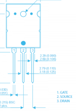
Exicon lateral MOSFETs are gate/source/drain pinout, not the same as other MOSFETs That layout looks wrong.
Okay thanks a lot!!
I could not find anything in the schematic but I have to be shown somewhere🙂
EDIT: found it🙂
I could not find anything in the schematic but I have to be shown somewhere🙂
EDIT: found it🙂
Attachments
Last edited:

did you export and re-import your actual netlist?Ehm confused!
I started by editing the schematic, to make the pin-numbers fit the mosfet's pin number I have selected. To my surprise did KiCad still tell me that I should place the traces in the same way as before. What have I done wrong?
Sorry for my late reply, did fall asleep... oops!🙂
But thanks a lot, and yes I did try that. Is the schematic correct or do you have to little information to judge that?
But thanks a lot, and yes I did try that. Is the schematic correct or do you have to little information to judge that?
Try redrawing the lines or use the mouse to move the symbol in the schematic to check everything is connected.
- Home
- Design & Build
- Construction Tips
- Worst PCB track-layout ever?