Wow! You've come so far in such a short time!
+1
Looking between your first design and your latest, you've taken on board a lot of suggestions and really made progress.
WOW!! Thanks a lot, it means a lot to me, you both says so!! 🙂
I'll look trough the advice's and try to correct the errors.
The only reason this has been and still are fun, is all due to all you who have replied, this is fun and I try to suck every bit of knowledge out of every comment.
The best part will be when I can turn on the amplifier and hear the first tones coming out🙂
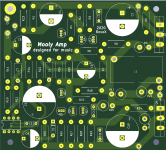
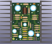
I have now changed some of the components, as advice, moved R5 a bit away to distance the gate and drain. I have also reduced the board's size by ½ inch in the bottom of the board (bottom of the picture). Some components did I also move to get shorter tracks.
The schematic is also updated according to a great advice in here.
If I look like I have ignored something, please ask, there are one of two reason for that, either I have made a stupid mistake or I have decided to keep something as it is. 🙂
Lastly have I tried to make a BOM. You can see that I have used an other type cap then specified on C8.
Wow what fun and great help from you all🙂
Attachments
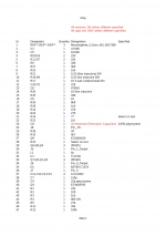


Where did C8 and that 'Polystyrene' tag creep into the mix 😀 I know part numbers got reallocated down the line as people drew their own circuits but I just wondered where it originated.
The original hand drawn circuit showed it as 22/50 meaning a 22uF 50 volt electrolytic and that was carried through to the software drawn diagram that replaced it in post #1 of the original thread 🙂
The original hand drawn circuit showed it as 22/50 meaning a 22uF 50 volt electrolytic and that was carried through to the software drawn diagram that replaced it in post #1 of the original thread 🙂
I am not sure where the faults did sneak in, but with 90% probability do I think I have the fault. I did all I could to copy every single symbol and text, but if there are errors, they could easily be due to my lack of knowledge.
When that is said, do my BOM look correct-ish or is that a mess?
Is there any other errors that have to be corrected?
When that is said, do my BOM look correct-ish or is that a mess?
Is there any other errors that have to be corrected?
R9 and R19 are 5W! Axial leaded they‘re big ones, please check and allow thermal clearance.
Output solder annular pads should be bigger.
Maximize supply tracks using copper plane.
JP
Output solder annular pads should be bigger.
Maximize supply tracks using copper plane.
JP
Your BOM is correct if all the parts are accounted for 😉
I think we said 3 watt was fine in practice for the 0.22 ohm resistors. These are what I used:
https://cpc.farnell.com/welwyn/w21-0r22-ji/resistor-ww-3w-5-0r22/dp/RE04656?st=resistors
Make sure that the TL071's you order are P-DIP outline which is plastic dual in line and not the little surface mount outline. The TL071ACP is DIP.
I did just find the smallest resistors that DigiKey had avaible, larger then 2W but thanks for the link to the resistor.
JPS64, thanks a lot, I have tried to placed the resistor away from other components, but near the mosfets. Great tip about the screw holes. 🙂
JPS64, thanks a lot, I have tried to placed the resistor away from other components, but near the mosfets. Great tip about the screw holes. 🙂
I don't know if my changes is for the better.
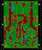
I have reduced the traces width from 4 mm to 3 mm, to make larger spacing between the traces. I have also moved the components around the mosfets, so they are nearer them. And maybe for the worse, have I moved the audio out to the fare top of the board.
I have reduced the traces width from 4 mm to 3 mm, to make larger spacing between the traces. I have also moved the components around the mosfets, so they are nearer them. And maybe for the worse, have I moved the audio out to the fare top of the board.
Attachments
Last edited:
Sorry I didn't think of it sooner -- large parts with flat bottoms (electrolytics) usually need to be bottom-side termination only. (I had to choke down this lesson the hard way when the technician building a prototype couldn't solder-in the pot-core inductors!)
Also, the smaller film types (in the little boxes) if you can't get the soldering iron under them.
Purdier and purdier . .
Cheers
Also, the smaller film types (in the little boxes) if you can't get the soldering iron under them.
Purdier and purdier . .
Cheers
Last edited:
I am just glad that you take your time to help!! 🙂
Sorry but I do not understand your comment about "bottom-side termination" and "pot-core inductors". I guess you are talking about the two pins, being between the board and the component, and therefore invisible from the component side, and therefore harder to "see" if soldered correctly?
Sorry but I do not understand your comment about "bottom-side termination" and "pot-core inductors". I guess you are talking about the two pins, being between the board and the component, and therefore invisible from the component side, and therefore harder to "see" if soldered correctly?
Sorry about the unnecessary info - 'pot core inductors'.
Any part whose body obscures where the lead comes out of the board. If there is component-side foil connecting those parts makes it harder to apply enough heat.
Also, just noticed -- some of the lead holes seem kinda big - mostly the output coil and 3W power resistors. The output trannies are probably the only thing that need such large holes - because they have the flat leads.
Happy to help such an eager, quick study 😉 You're doing great!
I know that I have made several versions of my first PCB ever but mostly has these changes been to implement your suggestions or to correct errors.
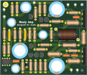
I have made a hopefully final design, where I have chosen to place each mosfet on opposite sides of the board.
May I please ask you if there are any errors, bad ideas that can harm the sound?
I have made a hopefully final design, where I have chosen to place each mosfet on opposite sides of the board.
May I please ask you if there are any errors, bad ideas that can harm the sound?
Attachments
Last edited:
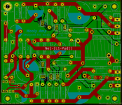
I would try and move the feedback take off point if possible.
You could cut the print where the red cross is and route the trace as shown in green. The point with the white arrow is where the feedback resistor should connect. It doesn't matter if you run a second trace here.
In other words the output line from the 0.22 ohm resistors should be a short track or spur with the feedback taken from that spur.
Try and make the layout be electrically like this... remember what we said about conductors (the print) having resistance and trying to make wiring and 'disappear'.
Attachments
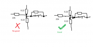
Look at this layout and see how the feedback take off point connects. It is probably one of the most important connection points in the whole amplifier. The exact point at which the 22k resistor connects is the only point where the output signal has been correctly sampled and the required feedback correction applied.
If the print had zero ohms resistance we would not have to bother... but it doesn't, it has definite resistance and so we need to make that 'disappear' by using the correct take off point.
If the print had zero ohms resistance we would not have to bother... but it doesn't, it has definite resistance and so we need to make that 'disappear' by using the correct take off point.
Attachments
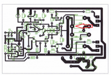
Look at this layout and see how the feedback take off point connects. It is probably one of the most important connection points in the whole amplifier. The exact point at which the 22k resistor connects is the only point where the output signal has been correctly sampled and the required feedback correction applied.
If the print had zero ohms resistance we would not have to bother... but it doesn't, it has definite resistance and so we need to make that 'disappear' by using the correct take off point.
Its also the inductance of the track which is about 1nH / mm.
It can quickly cause a phase shift and oscillation can occurr.
Keep feedback path as short as possible.
Coupling between tracks can be a problem, particularly if impedances are high... it might be interesting to try that in simulation sometime.
- Home
- Design & Build
- Construction Tips
- Worst PCB track-layout ever?