Oh thanks, that helped a lot, I did try to run a DRC on the schematic and it pointed at the spot with a missing connection thingy🙂
Originally had I used a standard (is there such a thing?) Mosfet component and when I changed to the right component, did I only rotate the component clockwise one time, move the lines a bit and did though I did reconnect them, but noooo, FAIL🙂
Originally had I used a standard (is there such a thing?) Mosfet component and when I changed to the right component, did I only rotate the component clockwise one time, move the lines a bit and did though I did reconnect them, but noooo, FAIL🙂
Please post your Kicad project files here. Those who use kicad can open them and give you advice. Without complete input from you, it will be difficult.
@FriedMule
First, drawing schematics:
- defining components
- RFS, MUSE bipolar, MKS/P capacitors
- CMF55 (0W5), CPF2 (2W), BPR58 (5W) resistors
- using 2SJ and 2SK Mosfets (TO3-P GSD)
I´ve a big library with components in different variants: pitch, mounting style and so on... all parts mapped to 3D models.
Then layout:
- placing UMS definition symbol
- placing first input connector: need to be central position so PBA could be simply rotated for R/L enclosure mounting
- placing power Mosfets according heat spreading
- placing power supplies Faston connectors
- placing output Faston connectors: supplies ground same as output ground
- placing all other components, and this is to do until you´re satisfied with the results: don´t forgot, good layout has an aesthetic look
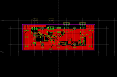
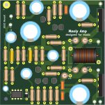
You find the results of one day hard working attached. It´s only ma proposal or my 2 cents.
JP
First, drawing schematics:
- defining components
- RFS, MUSE bipolar, MKS/P capacitors
- CMF55 (0W5), CPF2 (2W), BPR58 (5W) resistors
- using 2SJ and 2SK Mosfets (TO3-P GSD)
I´ve a big library with components in different variants: pitch, mounting style and so on... all parts mapped to 3D models.
Then layout:
- placing UMS definition symbol
- placing first input connector: need to be central position so PBA could be simply rotated for R/L enclosure mounting
- placing power Mosfets according heat spreading
- placing power supplies Faston connectors
- placing output Faston connectors: supplies ground same as output ground
- placing all other components, and this is to do until you´re satisfied with the results: don´t forgot, good layout has an aesthetic look
You find the results of one day hard working attached. It´s only ma proposal or my 2 cents.
JP
Attachments
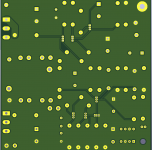
So finally do I think I have followed every of your advice's, hints and tips🙂
Until now has this been a lot's of fun and work, but I think I have reached the finish line. May I please ask you if you think that everything ok?
Until now has this been a lot's of fun and work, but I think I have reached the finish line. May I please ask you if you think that everything ok?
Attachments

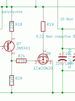
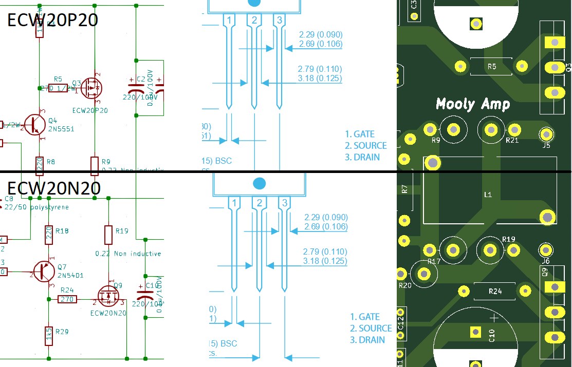
Q9, the lower N Channel FET needs to have pin 1 as the gate (correct), pin 2 which is the source should go to the negative rail (incorrect) and pin 3 which is the Drain going to the 0.22 ohm. So that pin is incorrect also.
Q3 which is the upper P Channel FET looks correct.
Q3 which is the upper P Channel FET looks correct.
Thanks a lot, I'd tried to change the connection from a normal mosfet to the special type. It was a recommendation🙂
Please how much of it is wrong?
Please how much of it is wrong?
Great so pin 1 shall point upward.Q9, the lower N Channel FET needs to have pin 1 as the gate (correct),
So pin 2 and 3 shall be switched.pin 2 which is the source should go to the negative rail (incorrect)
Ehm so eh so... pin 1 that was correct is not correct, because pin 3 shall be connected to the resistor that pin 1 is connected to?and pin 3 which is the Drain going to the 0.22 ohm. So that pin is incorrect also.
Sorry but I am now confused🙂Q3 which is the upper P Channel FET looks correct.
Glad that Q3 looks correct🙂
Oh now do I get it, I hope🙂
The symbol shall have pin 2 and 3 switched and then shall the symbol rotates so pin 3 connect to the 0.22 resistor?
The symbol shall have pin 2 and 3 switched and then shall the symbol rotates so pin 3 connect to the 0.22 resistor?
Yes 🙂
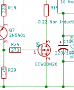
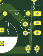
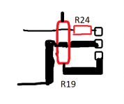
Try moving R24 closer to the FET.
Run the negative rail direct to the middle pin (pin 2)
Reposition R19 so it runs in front of the FET.
Try moving R24 closer to the FET.
Run the negative rail direct to the middle pin (pin 2)
Reposition R19 so it runs in front of the FET.
okay thanks, I'll do that instead! 🙂
What about R9, if you please?
EDIT: not enough space for that, do I think.
What about R9, if you please?
EDIT: not enough space for that, do I think.
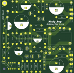
Attachments
Last edited:
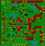
The board layout looks wrong for Q3 (the diagram was OK).
I'm assuming in all these that we are looking down on the board and so the gate (pin 1) is the top connection. The print is under the board.
It's easy to go cross eyed working with images... make sure they are correct 🙂
I'm assuming in all these that we are looking down on the board and so the gate (pin 1) is the top connection. The print is under the board.
It's easy to go cross eyed working with images... make sure they are correct 🙂
Attachments

Wow! You've come so far in such a short time! 
Just a couple bits, maybe 'for the next iteration' would be plenty soon enough:
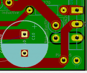
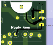
The new position of R9 will probably be just fine. But as a general policy, having a little more space between Gate and Drain connections is better. The driven end (lower in the pic) of R9 is relatively low impedance so it'll be OK in this instance. The other end - connected to the Gate - is the trace that Mooly suggested to shorten -- the high impedance of a MOSFET input makes it too eager to receive signals capacitively coupled. Even though the 270R R9 will control it, the Drain pad can swing almost rail to rail.
While most electrolytic capacitors are polarized, most others are not. C13 could be either, by the value (larger values are more likely to be electrolytic), but the pics look more like an electrolytic has been specified. If so, the polarity is backwards: The inverting input of the opamp will be very close to ground; the other end (connected to the opamp output) will live a few volts below ground depending on the gains of Q6 and Q8.
You might also want to remove the polarity symbol from C7, C4, C3, C11 and C12. C8 is a special case: Having the '/50' voltage rating suggests electrolytic, which would be more likely for that spot in the circuit than 22 pF polystyrene. (22 uF / 50V electrolytic instead.) I read the earlier posts, but I don't remember -- worth checking?
Still, I am really impressed with how you've sunk your teeth into this -- an admirable undertaking -- and its looking darn fine!
Cheers
Just a couple bits, maybe 'for the next iteration' would be plenty soon enough:
The new position of R9 will probably be just fine. But as a general policy, having a little more space between Gate and Drain connections is better. The driven end (lower in the pic) of R9 is relatively low impedance so it'll be OK in this instance. The other end - connected to the Gate - is the trace that Mooly suggested to shorten -- the high impedance of a MOSFET input makes it too eager to receive signals capacitively coupled. Even though the 270R R9 will control it, the Drain pad can swing almost rail to rail.
While most electrolytic capacitors are polarized, most others are not. C13 could be either, by the value (larger values are more likely to be electrolytic), but the pics look more like an electrolytic has been specified. If so, the polarity is backwards: The inverting input of the opamp will be very close to ground; the other end (connected to the opamp output) will live a few volts below ground depending on the gains of Q6 and Q8.
You might also want to remove the polarity symbol from C7, C4, C3, C11 and C12. C8 is a special case: Having the '/50' voltage rating suggests electrolytic, which would be more likely for that spot in the circuit than 22 pF polystyrene. (22 uF / 50V electrolytic instead.) I read the earlier posts, but I don't remember -- worth checking?
Still, I am really impressed with how you've sunk your teeth into this -- an admirable undertaking -- and its looking darn fine!
Cheers
Last edited:
- Home
- Design & Build
- Construction Tips
- Worst PCB track-layout ever?