FriedMule, 10 hours is nothing 😉 I think when I did my first boards I spent probably a couple of months (with a few hours a day) before I got something I was happy with. Part of that was the learning curve for KiCad but also a lot of it was because I felt I could do better.
If using KiCad do use the error checker.
Tony.
If using KiCad do use the error checker.
Tony.
Okay I thought that 10 hours were insanely slow, but that's a comfort that it takes time🙂
I'll try to use the error checker.
My biggest "slow down" is when a component is not avaible in KiCad.
I do like Micro-cap but it can't do pcb design.
I'll try to use the error checker.
My biggest "slow down" is when a component is not avaible in KiCad.
I do like Micro-cap but it can't do pcb design.
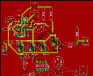
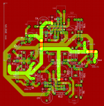
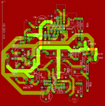
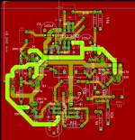
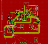
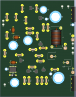
I'll post pictures below to show evolution of my board. The first pic is when I first started and had not placed all of the parts. The second was apparently iteration two. Third iteration three, some are skipped (didn't take a snapshot apparently) they get more subtle towards the end. The last is what is probably the final version of the board that I settled on.
This was over a period of about a month, with probably more hours a day spent on it than I care to admit.
The circuit works and is in daily use 🙂 I went with quite thick traces and decent sized pads. The board is 10cm square.
Not posting this as an example of good design, it's probably still got a lot of things that could be better, but to show an evolution from beginning to do layout, to the final result 🙂
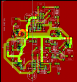
Interestingly I named the very first pic horrid_layout 😀 so I was feeling the same as you were when you wrote the title for this thread 😉
The last one is to show that I did actually make it and complete it. Something that is somewhat of a rarity in the Wintermute household. 😉 Admittedly it was around 6 years from initial inception of the idea to the final thing being built but the important thing is that it got completed 🙂
Tony.
This was over a period of about a month, with probably more hours a day spent on it than I care to admit.
The circuit works and is in daily use 🙂 I went with quite thick traces and decent sized pads. The board is 10cm square.
Not posting this as an example of good design, it's probably still got a lot of things that could be better, but to show an evolution from beginning to do layout, to the final result 🙂
Interestingly I named the very first pic horrid_layout 😀 so I was feeling the same as you were when you wrote the title for this thread 😉
The last one is to show that I did actually make it and complete it. Something that is somewhat of a rarity in the Wintermute household. 😉 Admittedly it was around 6 years from initial inception of the idea to the final thing being built but the important thing is that it got completed 🙂
Tony.
Attachments
-
 horrid_layout.png38 KB · Views: 192
 -
 Synergy_completed.JPG649.3 KB · Views: 126
 -
 synergy_layout_11.png50.3 KB · Views: 111
 -
 synergy_layout9.png62 KB · Views: 60
 -
 synergy_layout8.png59.6 KB · Views: 55
 -
 synergy_layout7.png61.2 KB · Views: 55
 -
 board5.png51.3 KB · Views: 157
 -
 board4.png50.4 KB · Views: 160
 -
 board3.png50.8 KB · Views: 160
 -
 layout_2.png33.2 KB · Views: 180
My biggest "slow down" is when a component is not avaible in KiCad.
......
If a board is only for your own use then having the proper outline isn't always important. As long as you have correct dimensions of the real part then you can just use separate pads and place them manually.
If devices like the Lateral FET's aren't in the parts library then use something else of the same style such as an IRFP9240.
wintermute thank you a lot for sharing the pictures! Lol so you felt like I did when starting🙂 Ok I did mostly feel like a slow mule, looking down in into an engine room for the first time🙂
Finally is all the components placed, the verticals do not look like that but they are carbon 0.22 resistors. The board is still same size but I expect it to get a lot smaller, after tracing.
Every resistor pad is 4 mm (157.5 mil).
That looks very neat 🙂 There is no problem with mounting those parts vertically if it helps the layout.
Fantastic, great, I find this very funny, interesting and exiting! Even I have, again, just spend about 5 hours🙂
Worth every second!
Worth every second!
Attached. It is in Eagle though. There are points I would change. The groundplane might be switched to the top for example. Beware also that there is a smd resistor position under the board. It allows to either connect the power ground and the signal ground on the board or at the PSU, depending on your grounding choices.Dear 00940, Can you kindly post the project files for your layout of the mooly amp ? Both schematic and pcb ? I think it is in kicad !--gannaji
If I were doing a pcb for myself, I think I'd want to put an output relay and circuitry for delay/dc protection directly on the board, as they are essential to the design.
It is possible, depending on how you wind it. A good explanation here : Inductive vs. Non-Inductive Resistors - FAQs - Engineering and Component Solution Forum - TechForum │ Digi-KeyWhile selecting components I search a lot in the original thread about Mooly's fantastic amplifier and some of the resistors have to non inductive = not wirewound, and that do make a lot of cense. But then do I stumble upon non inductive wirevound resistors??!! An inductor that is non inductive??
On the PCB topic, it is also good to clarify what will be your method of production. For homemade pcb, tracks and pads have to be oversized, to facilitate production. If you send your gerbers to a PCB fab, then you can have smaller pads and tighter tolerances. 4mm pads for 0.6W resistors is a bit much, as that will complicate running tracks in between the pads. For such resistors, I've got about 1.27mm diameter pads for commercial production and I would up that to about 2-2.5mm for home made pcb. This said, places like jlcpcb are so cheap these days that I haven't etched a pcb in while.
Attachments
No doubt in that I'll order the PCB🙂 -If you add together the cemicals, trays, transfermethodes and my now zero seconds long expirience, it can only be cheaper and better to order🙂
A noob question: am I right in assuming that shorter and more narrow tracks gives a lower impedance then greater width but longer traces?
What I am thinking of, is if it's not better to place the components as tight as possible with traces that have same with as the pads, instead of space the components out, to get room for 2 x pads width in tracks?
I think this tutorial would really help you : PCB Design & Layout Tutorial - Learn how to design a professional PCB! Scroll down and download the pdf, it's a good read, covering a lot of basics.
...But then do I stumble upon non inductive wirevound resistors??!! An inductor that is non inductive??....
A "winding" is not always inductive.
Attachments
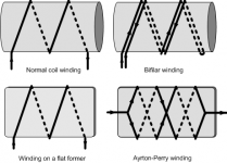
It was standard practice at the time to state 'non inductive' against such resistors on circuit diagrams. The 10 ohm resistors in the output network should ideally be either carbon or metal film. The 0.22 ohm will be a couple of cm of resistance wire wrapped around a former and so any inductance is virtually non existent.
If it were a 10k or even a 100k wirewound then inductance becomes much more significant, particularly in high frequency circuitry... and such parts do exist.
You would never use wirewound resistors in a tuner for example.
If it were a 10k or even a 100k wirewound then inductance becomes much more significant, particularly in high frequency circuitry... and such parts do exist.
You would never use wirewound resistors in a tuner for example.
I have chosen this https://www.digikey.com/products/en?keywords= FCR3WSJT-73-10R for the 10 Ohm.
Have an idea of Carbon being better, but I have never heard about Yageo, is that quality or a cheap brand?
Have an idea of Carbon being better, but I have never heard about Yageo, is that quality or a cheap brand?
It says non in stock for me...
Have a look at these:
ROX3SJ10R TE Connectivity Passive Product | Resistors | DigiKey
Have a look at these:
ROX3SJ10R TE Connectivity Passive Product | Resistors | DigiKey
- Home
- Design & Build
- Construction Tips
- Worst PCB track-layout ever?