Thanks Mos57....wow lot of power....27ma for JFETs? wow i don"t have that kind of Jfet to use...i may parallel 4 or 5 K170 for each, How about using a mosfet say IRF610 or any other alternatives?
you use irf9540 more than 4v zener is needed,,,the j162 is lower vgs so you use 3v for 2.11A idle. Is this idle current 2.11a per Vfet or or for the 2?
What should be the minimal VA rating of my PSU for 2Channel (stereo).
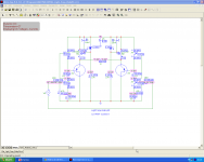
Question on the topology: why not have J1 and J3 share a common source resistor and be a real differential amplifier?
Regarding MOSFET CCS - good luck getting simulated results out of a J162 in that configuration, that will only work in a simulator. Also, that configuration will not work properly with IRFP anything - they have positive temperature coefficient. How about re-simulating your schematics at a temperature other than default? As shown you can expect variations in current in the range of at least 1:3 (and I'm being optimistic here) if you stick in a randomly chosen J162. If the schematic was 'inverted' and you used K1058, the situation would be a bit better but not much. What you need there is a 'ring of two' CCS, that has a source resistor and controls the MOSFET via a BJT whose B-E junction is across the source resistor keeping it's voltage at around 0.6V or so. This will be somewhat temperature dependant (negative - higher temp, lower current) because Vbe of the control BJT will ddrop if it heats up from the surrounding parts which do generate a lot of heat. However, the current becomes independent of the MOSFET type (and you could even use a BJT darlington).
As I've said in another thread, laterals do vary quite a bit between instances of the same part, and P-ch varies about 3x more than N-ch. At least that's my experience from testing some hundreds of them to get almost perfect matched sixes (3 P, 3 N) (a total of about 20kg of lateral MOSFETs!). It is unwise to rely on MOSFET Vgs treshold in any real world application, I suppose no-one wants to buy 10x the required number of parts just to select for it (or some 20-30x if P-ch).
PS you could also make the CCS adjustable (but only using laterals) by replacing the cener with a TL431 shunt regulator set with a trim pot.
@MOS57 - distortion spectrum displays on a linear scale are really completely useless.
Last edited:
Thanks ...yes 13 of my J18's are of the same rank..
using a center tapped former is a very nice option since i do have a autotransformer (stepdown 220 to 110, 750Va) can I use this thing without making a gap?
You should be able to use something like a secondary of a regular transformer, for good LF extension look at about 2x the actual voltage and 4x the actual power, so say a 50VA or so transformer with 2x24-30V secondary. If it's a classical EI or C core, no special gapping should be needed assuming you carefully balance the currents in the left and right VFET, in this case the easyest way would be to select them into pairs.
The schematic would have to be changed - instead of the CCSs, the total center-tapped winding goes across the load (from S to S of the VFETs), the center tap goes to a supply voltage for the VFETs which can now be quite a bit lower (20-22V or so). However, the drains of the driver JFETs need to still be on a voltage higher than this as this defines the bias and maximum excurcion voltage for the VFETs. In fact in this topology this voltage quite severely limits the maximum swing on the output, as it is possible to almost completerly turn on the VFET but not to tuen it off. And - what actual swing you will get will depend VERY much on the VFET rank. Unfortunately, the JFET stage is limited in supply voltage to some 40V max as this is the guaranteed Vdsmax for the JFETs. The drain voltage of the JFET driver stage also defines the bias for the VFETs, this needs to appear before the main supply that goes to the center tap of the autoformer. The current schematic has the advantage that the bias is set automatically by the CCSs. For the autoformer version it is also possible to do something like that by tying a CCS in series from the center tap of the autoformer to the power supply, the center tap needs to be decoupled to GND with a large cap, and unless it's supplied from a lower voltage than the drivers, it will produces heat losses. The CCS and capacitor insure that the VFETs are protected from no bias conditions.
Last edited:
Thanks ILIMZN for the new suggestions...I do have 2x25v/80VA Toroid trafo with 220vac primary....so i will just use the secondary winding which has lower winding turns (inductance)?
Having CCS between Ctap and PS should have at least 5A current flowing so my CCS should be able to produce this...
Other option is the ccs using a darlington BJT? a I also have some ONsemi Darlintong BJT's.
Hi mos57...any update..how about other variation as suggested? Thanks
Having CCS between Ctap and PS should have at least 5A current flowing so my CCS should be able to produce this...
Other option is the ccs using a darlington BJT? a I also have some ONsemi Darlintong BJT's.
Hi mos57...any update..how about other variation as suggested? Thanks
Were raised a bit of questions. I will try to answer one at a time in the following posts.
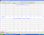
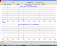
We start from the charts of the distortion. Linear level of harmonics show at first glance (more intuitively) the relationship between the various grade of harmonics. In fact, the charts posted before immediately detects that the only noticeable distortions are those of the third harmonic.
The other with respect to the latter are practically negligible.
However,for those who want a more detailed analysis, I repeated here the graphs for the version with the CCS that seems the most interesting.
The attached pictures are referred to respectively 12 -10 - 4 - 1 Watts - @ 8 Ohm load
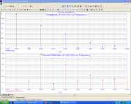
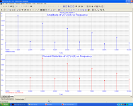
Attachments

Last edited:
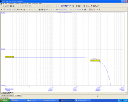
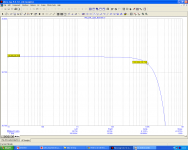
Another issue raised is the variation of the current of the output stage with the variation of temperature. This variation is supposed to be very high and therefore very dangerous condition of operation.
As you can see from the attached graphs the output current varies (decreases) of about 10 mA for an increase of 10 degrees (27 to 37), while from 37 to 47 degrees the current drops another 94 mA. I do not think so disastrous behavior and the behavior in every way that I would describe as "conservative."
In each case the observations to improve the performance must be taken into account and in the following I will post a first variant that improves this behavior by making the current more stable.
Pictures are referred to a default temp of 27° then 37° then 47° for comparison
Attachments

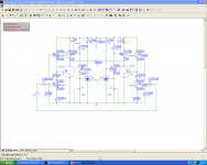
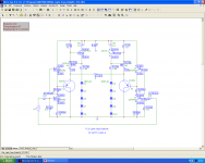
Here I show the variant to stabilize the current vs. temperature. The zener were replaced with simple PNP CCS polarized with 2 diodes. The resistors 390 Ohm on emitters can be replaced with potentiometers from 500-1000 Ohm allowing to adjust the right value of the current generated also not disposing of selected pairs of MOSFET. Another option would be the use of the TL431 as suggested.
In the same conditions of temperature variations of the previous case (from 27° to 47°). here the change is 21 mA. You could do better but I prefer not to go beyond this value because in the practical application is a guarantee for better security.
I also added graphs for more 10° down (17°) and 10° high (57°)
Attachments
-
 TC_Light_Srpp BabySit_Dynamic_DC_Analisys_27°.png49.8 KB · Views: 123
 -
 TC_Light_Srpp BabySit_Dynamic_DC_Analisys_37°.png47.8 KB · Views: 106
 -
 TC_Light_Srpp BabySit_Dynamic_DC_Analisys_47°.png48.4 KB · Views: 93
 -
 TC_Light_Srpp BabySit_Dynamic_DC_Analisys_17°.png47.6 KB · Views: 86
 -
 TC_Light_Srpp BabySit_Dynamic_DC_Analisys_57°.png47.7 KB · Views: 104
Of all design..which of them is more stable? I don't see the tl431 variant...maybe next. thanks for kind effort simulating those schematics...
Of all design..which of them is more stable? I don't see the tl431 variant...maybe next. thanks for kind effort simulating those schematics...
All these designs are very stable. They have low efficiency but are solid as a rock. We have to agree to get what you mean by stable.
If we mean that the operation is "safe" from an electrical standpoint , namely that reliable and not subject to breakdowns for anomalies that may be generated during operation, in this sense, then all the circuits presented in this thread are at the highest levels for the following main reasons:
- absence of feedback
- absence of reactive elements
- a single power supply
- power devices that have a zero or positive temperature coefficient (in them the current decreases with increasing temperature).
Moreover, the presence of CCS in some of them is an additional degree of protection.
An amplifier more stable? An amplifier that is power off 😀
If instead for stable we includes an amplifier that maintains in the time and at different temperature the same operating conditions (which the value of the output current) then is a different matter.
In the case of circuits presented here the one that best fulfills this condition is the schematic with mosfet powered by BJT ccs (last one of the previous schemes).
However, paradoxically, those in which the current varies, being that it decreases as the temperature increases are to be considered safer especially those with load resistors.
We come to the second point: why had not yet submitted a circuit with TL431.
These devices were invoked to allow a continuous adjustment of the bias voltage, such as to adapt to mosfet with different Vgs. This is the only advantage that their presence provides.
In fact, from a point of view of stability of the current Vs temperature the situation is even worse than in the case of the circuit with the zener, as you can see from the simulations attached. The lat Mos as mentioned have a drain current which decreases at rising temperature. What serves us to counter this effect is a gate voltage that must increase with increasing temperature. All contrary for vertical mosfet
Being instead the TL431 a ccs quite accurate even varying the temperature parameter, it follows that the gate voltage of the MOSFET remains stable kilter the compensatory function.
Schematic attached with TL431 are referred to 27° 37° 47° for direct comparison.
Attachments
In the previous post, in the list of the highlights that make this type of amplifiers particularly stable, I forgot to mention the use of the automatic bias for Vfet.
This means that any variation of current through the Vfet be felt directly by the gate of the same as voltage with opposite polarity to that of the source current, for which the effect is to offset and limit this variation.
What I like least of these circuits?
They do not work in class B (AB)
Vfet not have voltage gain.
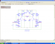
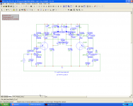
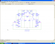
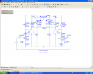
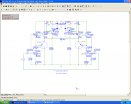
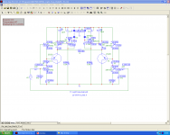
Question on the topology: why not have J1 and J3 share a common source resistor and be a real differential amplifier?
Well, I had not yet shown the circuit with differential input stages (LTP) for two reasons.
- For those who wanted an unbalanced input, I was thinking to use my phase shifter that is better balanced compared to 'LTP although the latter is easier to implement.
- I suspected, as then it is confirmed by the analysis attached, a small performance degradation in both distortion and frequency response.
In the analysis of the distortion of the individual harmonics it is clearly seen that those of odd order remain exactly the same, while those of even order are higher compared to the basic circuit.
For convenience I attach the wiring diagrams, analysis distortion (@12W) and frequency response of the two circuits.
As you can see the comparison was made at par, ie under the same operating conditions.
Attachments
-
 Light_Srpp BabySit.png46.4 KB · Views: 357
 -
 Light_Diff_Srpp BabySit.png44.1 KB · Views: 365
 -
 Light_Srpp BabySit_Log_Distortion_Analisys_12W.png55.2 KB · Views: 343
 -
 Light_Diff_Srpp BabySit_Log_Distortion_Analisys_12W.png56.4 KB · Views: 335
 -
 Light_Diff_Srpp BabySit_Comp_Log_Distortion_Analisys_12W.png148.3 KB · Views: 323
 -
 Light_Srpp BabySit_AC_Analisys2.png46 KB · Views: 104
 -
 Light_Diff_Srpp BabySit_AC_Analisys2.png46.8 KB · Views: 94
Last edited:
In the previous post, in the list of the highlights that make this type of amplifiers particularly stable, I forgot to mention the use of the automatic bias for Vfet.
This means that any variation of current through the Vfet be felt directly by the gate of the same as voltage with opposite polarity to that of the source current, for which the effect is to offset and limit this variation.
What I like least of these circuits?
They do not work in class B (AB)
Vfet not have voltage gain.
I presume that the supply voltage is regulated.
2SJ18 has a mu of 4..very little gain so expected that the jfets has to run higher current....i dont have 2n4392 Jfets...i do have small jfets like K117,K246 and k170. What other alternatives?
I also want to see the unbalanced input circuit..
Hello, you can use:
2N5486
BF246
BF247
J310
or 2 pairs connected in parallel:
2SK163N
2SK140V
2SK363V
2SK371V
2SK372Y
J111
BF245C
You can use regulated or unregulated PSU.
I will do an unbalanced input for only one type of schematic. I not have seen definitive choiche by You.
Transformers in this follower configuration not have much sense for me, since we use autobias and one single PSU, but there is an option in common source outstage. Stay tuned. 😎
Hello, you can use:
2N5486
BF246
BF247
J310
or 2 pairs connected in parallel:
2SK163N
2SK140V
2SK363V
2SK371V
2SK372Y
J111
BF245C
You can use regulated or unregulated PSU.
I will do an unbalanced input for only one type of schematic. I not have seen definitive choiche by You.
Transformers in this follower configuration not have much sense for me, since we use autobias and one single PSU, but there is an option in common source outstage. Stay tuned. 😎
Junm, looking at current I have forgot of max power.
Delete the list above, sorry.
This is the right list:
single devices
2N5487
2N5488
U1715
two devices in parallel
2SK163N
2SK363V
J111
BF246
BF247
Here I show the variant to stabilize the current vs. temperature.
Temperature variations come down to zener tempco and anyway should not be a bog problem unless you were driving your VFETs at the maximum possible dissipation, but then you would still have the problem of different ambient temperature 🙂
At the suggested current the MOSFETs have a negative tempco (I wonder if the models accurately model this!). Still, as I said, putting a zener in G-S and sticking in a J162 you just bought will give you nice lottery numbers for the CCS current. You will either need to select MOSFETs or get a 'variable zener' (TL431, or use a different style CCS (with source resistor for the MOSFET).
a little bit confused, will it be better by using a fixed zener and a resistor on J162 source.
@Mos57 have you tried this option?
@Mos57 have you tried this option?
a little bit confused, will it be better by using a fixed zener and a resistor on J162 source.
@Mos57 have you tried this option?
I think your confusion stems from the fact that ILMZN took the words of the post No. 107 and then comment the schematics of the post 106.
In the figures of the post 106 are not present trimmer to adjust the value of bias of 2 mosfet with different Vgsth , trimmer whose use has been suggested, though not shown in the diagrams of the post 107.
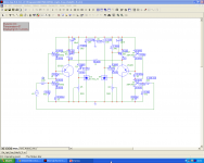
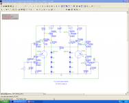
Today, however, I introduce a scheme with compensation for the effects of temperature in which as seen from the attached analysis of the output currents it varies of 1 mA in a range between 17 and 57 degrees in temperature.
The bias current is set by the trimmer X3 and X4, while the rate of temperature compensation is set by resistors 1.13 K (they also replaceable by other trimmers).
Notes: A resistor value lower than that shown produces undercompensation, while a higher value produces overcompensation.
Of course, in the real case will end a calibration procedure to locate the right setting value.
Attachments
-
 TC_Light_Srpp BabySit_Dynamic_DC_Analisys_17°.png49.1 KB · Views: 105
 -
 TC_Light_Srpp BabySit_Dynamic_DC_Analisys_27°.png48.9 KB · Views: 98
 -
 TC_Light_Srpp BabySit_Dynamic_DC_Analisys_37°.png49.5 KB · Views: 91
 -
 TC_Light_Srpp BabySit_Dynamic_DC_Analisys_47°.png47.3 KB · Views: 88
 -
 TC_Light_Srpp BabySit_Dynamic_DC_Analisys_57°.png47.3 KB · Views: 104
Last edited:
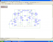
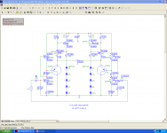
In these days I have developed a new approach to control the output current and stabilize it against temperature variations.
I want to show the circuit because personally I prefer it.
Here, unlike the previous scheme, there is the monitoring of the current through the two 0.22 Ohm resistors.
X3 and X4 set the output bias current
Thermal compensation is carried out mainly by the germanium diodes D1-D10.
A lower number of diodes overcompensate while a greater number overcompensate .
It can also be used the diodes 1N34A type of easy availability on Ebay.
From attached pictures you can see that the current of the output stage varies only 1 mA (0.0475%) within an extended range of temperatures between 7 and 67 celsius degrees.
Attachments
-
 TC2_Light_Srpp BabySit_Dynamic_DC_Analisys_7°.png47.2 KB · Views: 119
 -
 TC2_Light_Srpp BabySit_Dynamic_DC_Analisys_17°.png48.6 KB · Views: 99
 -
 TC2_Light_Srpp BabySit_Dynamic_DC_Analisys_27°.png48.7 KB · Views: 91
 -
 TC2_Light_Srpp BabySit_Dynamic_DC_Analisys_37°.png48.7 KB · Views: 77
 -
 TC2_Light_Srpp BabySit_Dynamic_DC_Analisys_47°.png47.3 KB · Views: 95
 -
 TC2_Light_Srpp BabySit_Dynamic_DC_Analisys_57°.png47.2 KB · Views: 94
 -
 TC2_Light_Srpp BabySit_Dynamic_DC_Analisys_67°.png48.5 KB · Views: 100
Last edited:
A lower number of diodes overcompensate while a greater number overcompensate .
Errata corrige:
A lower number of diodes UNDERcompensate while a greater number overcompensate, of course. 😎
- Status
- Not open for further replies.
- Home
- Amplifiers
- Solid State
- What to do with this Sony V-FETS?