Schemes are simple diagrams with a simple representation of the electric circuit . So my plans are essential as well as the other schemes are essential where there are not more detailed descriptions.
There are other forms for more detailed analysis such as articles, web pages or forums.
In this regard, for the most distracted people long time ago on this forum I opened the following threads:
the first Vfet single ended amplifier presented here (not an half amplifier...)
http://www.diyaudio.com/forums/pass-labs/154009-2sj28-vfet-se-amplifier.html
The first Vfet amplifier in TRANSNOVA configuration.
http://www.diyaudio.com/forums/solid-state/166143-new-complementary-v-fet-amp-best-past.html
I also remember that I was the first to warn this community when there was the possibility to buy on Ebay those precious Vfets
http://www.diyaudio.com/forums/solid-state/150299-nos-vfet-sale-ebay.html
Excuse me if I took off a few stones underfoot. 😀
Best regards, Francesco.
Shinichi Kamijo designed some SIT/VFET amplifiers and some of them are reprinted to the internet including this site.
Evolve Power Amplifiers
He explained the effect of power supply ripple on triode and equipped canceling circuit in his SIT amp.
Power Sauce Drift Cancel
He designed only one amp with complementely SEPP with J27/77 but others are circlotron.
(Circlotron is so to be called as Cross Shunt Push Pull :CSPP in Japan.)
He died last year but his website is managed his brother today.
Shinichi Kamijo was a great designer and an innovator.
His work was that of the rediscovery and re-use in audio circuits of the SIT and he was a popularizer of the CSPP in solid state and many other interesting circuits. A true master!
I am very sorry to learn of his death.
His website is included from the beginning in my links page and I'm proud.
A great man.
In the past we have exchanged emails and thanks to him my hope in the sit was reborn.
A greeting of respect to his brother that is keeping alive the website
Yes, it's separate PSU. I chose 20V to supply the JFET (I wanted JFET's drain at half of the V2 voltage and 10V to bias the VFET, in order to get 1A bias through it). V1 is 19V because it was convenient - it's standard value for laptop PSUs which are cheap and abundant and it suits my power and heatsink requirements. V2 needs to supply only about 10mA per channel. Each channel should have its own V1 which can be of higher voltage and/or current (depending on your speakers and power demands) but, as ilimzn said, don't go over 30W of thermal dissipation per VFET.
thanks juma....I do have some laptop psu to ry first before going 24 v...it happens that have several 24.5 v/(5-10A) Smps to use so i want to use 2 in series and isolate the chassis ground from it. I will try to parallel 2 pcs of J18so a not to over drive the SITS.
I wholeheartedly agree! The CSPP amp schematic is a good start, with a bit of jiggling around the ground references it can have complete symmetry and still be quite simple (except for a number of power supplies - but CSPP always have that 'problem'). Again, it's also possible to use a center-tapped autoformer in such a design to get the VFETs into the more voltage, less current more linear areas, and in this case the added bonus is that the DC currents in the autoformer cancel out. Since the required inductance and ratio is low, assuming one takes care of DC balance, this could be even wound on a toroid core and offer quite high performance. Ah, so many ideas, so little time 😛
This is really my first target but i just can't get the k213/k214/k215 at local stores here, may try ordering in ebay... One qouestion does it need separate trafo's with separate multiple winding as indicated in the psu schema or can I just use one for for both channels?
http://www.diyaudio.com/forums/pass-labs/154009-2sj28-vfet-se-amplifier.html
Best regards, Francesco.
You use J28 in your SE design and another Sit K79 on the front end and BJT on the driver. will it suit J18 and say a Jfet Input say K373 a 100v Jfet as Front end (input), what are the possibvle changes?
Hi
please look what great potential has this topology:
Harmonic Frequency Fourier Normalized Phase Normalized
Number [Hz] Component Component [degree] Phase [deg]
1 1.000e+03 5.464e+00 1.000e+00 -0.21° 0.00°
2 2.000e+03 5.437e-04 9.951e-05 -82.57° -82.36°
3 3.000e+03 2.502e-04 4.579e-05 26.27° 26.48°
4 4.000e+03 1.901e-06 3.480e-07 -158.70° -158.49°
5 5.000e+03 2.493e-06 4.563e-07 -134.52° -134.31°
6 6.000e+03 5.199e-08 9.515e-09 35.90° 36.11°
7 7.000e+03 3.657e-08 6.692e-09 59.92° 60.13°
8 8.000e+03 1.078e-09 1.973e-10 -135.99° -135.78°
9 9.000e+03 5.980e-10 1.095e-10 -87.74° -87.53°
Total Harmonic Distortion: 0.010954%
Good performance from a lateral Mosfet...Just dunno if applicable to Vfets....but one of the Design of Kamijo uses Lateral Fets in a circlotron.
You use J28 in your SE design and another Sit K79 on the front end and BJT on the driver. will it suit J18 and say a Jfet Input say K373 a 100v Jfet as Front end (input), what are the possibvle changes?
You can use 2sk373 as second choice .
Remember to decrease the value of source potentiometer to 1K.
Other altenative high voltage jfet are here: CRYSTALONICS | semiconductor manufacturer of Small Signal Transistors, JFETS, DUAL TRANSISTORS, QUAD TRANSISTORS, POWER TRANSISTORS, CURRENT REGULATOR DIODES, VARACTOR DIODES and custom HYBRID MICROCIRCUITS
If you want to use the 2SJ18 brings the voltage of the output stage around 30 volts. The power will come down to around 6 Watt
Thanks MOS57..Once I wind my Choke i will try this as well as Juma's Design and see which is better for my ears. These are class A so need also a very good and big heatsinks and stiff power supply preferably regulated.
Are there any schematics that are more Efficient? I want to get at least 15w of classA and 30w AB with this Vfets.
Are there any schematics that are more Efficient? I want to get at least 15w of classA and 30w AB with this Vfets.
Thanks MOS57..Once I wind my Choke i will try this as well as Juma's Design and see which is better for my ears. These are class A so need also a very good and big heatsinks and stiff power supply preferably regulated.
Are there any schematics that are more Efficient? I want to get at least 15w of classA and 30w AB with this Vfets.
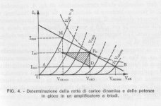
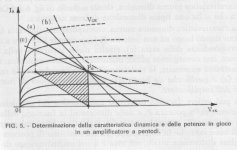
The performance of a Vfet amplifier is, similarly to that of the triodes, very low.
The poor performance is due to the shape of the output characteristics that do not allow large voltage excursions.
In particular, the minimum voltage reached is significantly higher than that of a comparable pentode or transistor stage. (See the two attached images)
In that the useful power is represented by the triangle.
If you want to obtain a power of 30-35 watts I suggest a underpowered version of my 100 watt circlotron.
A 40+40 V power supply for the output stage and +/-30 volts power supply voltage for the driver circuit should be sufficient. For the input folded cascode 2N4401/2N4403 is a good choice. 😉
Also resistors must be recalculate !!!
Best regards
Attachments
Last edited:
Hi Nmos, are those loadlines for K60?
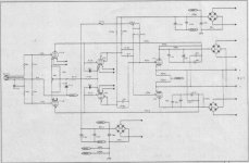
Are you referring to this http://www.amplimos.it/images/SIT CIRCLOTRON AMP 100.bmp
it uses the powerful k180 n ch Sit....How about using all J18 Pch SIT ?
Are you referring to this http://www.amplimos.it/images/SIT CIRCLOTRON AMP 100.bmp
it uses the powerful k180 n ch Sit....How about using all J18 Pch SIT ?
Hi Nmos, are those loadlines for K60?
Are you referring to this http://www.amplimos.it/images/SIT CIRCLOTRON AMP 100.bmp
it uses the powerful k180 n ch Sit....How about using all J18 Pch SIT ?
The graphs posted are related to generic triode (similar to V-FET) and generic pentode (similar to MOSFETs and bipolar transistors).
On my website you can still find the curves of 2sj18 and other v-fet that I have measured.
Unfortunately my curve tracer is for small signal devices and not very suitable for precise measurements of power devices. It seems that ILLZMAN is equipped with a professional curve tracer . Having the 2SJ18 he could measure and post the pictures.
But to understand the concept expressed in the previous post, also referring to the image downloaded from the site, and removing the first three curves to the left (area just not linear), then drawing on it the load line , we can see that the minimum voltage will not be less than 8 - 10 Volt about.
Therefore the maximum excursion of the signal will be less than it with respect to the power supply voltage. It follows that to obtain the right excursion we must move the operating point 10 volts to dx (more) and therefore the power supply must generate 10 volts more than necessary.
So the stage employing a Vfet must be powered at a higher voltage than equivalent transistor or mosfet stage and this more voltage is wasted.
It makes vfet stage less efficient than other devices.
The answer to the second question is: yes, I am referring to this.
You can use this scheme simply by reversing the polarity of the batteries and the polarity of the transistors and caps:
input's transistors: 2N4403
folded cascode transistors: 2N4401
follower transistors: 2N4033 ( complementary to 2N3019).
circlotron Stage transistors: 2SJ18.
ccs transistors: 2N4033 and 2SA970 (complementary to 2SC2240).
Last edited:
Thanks MOS57, I know a little about triode and pentodes loadlines so i can have a basis on power calculation and VGS with respect to idle current by the curves on their datasheets.
I had also in mind about having a PP tube amps with triodes on the input and phase splitter and vfets as output stage but with out OPT and +/- Supply Voltage for the output Vfets, will this be possible without OPT?
I had also in mind about having a PP tube amps with triodes on the input and phase splitter and vfets as output stage but with out OPT and +/- Supply Voltage for the output Vfets, will this be possible without OPT?
Thanks MOS57, I know a little about triode and pentodes loadlines so i can have a basis on power calculation and VGS with respect to idle current by the curves on their datasheets.
I had also in mind about having a PP tube amps with triodes on the input and phase splitter and vfets as output stage but with out OPT and +/- Supply Voltage for the output Vfets, will this be possible without OPT?
It is possible the direct coupling without interstage transformers
.
The driver circuit must be powered with a dual voltage PSU, so that output from the driver have the bias voltage for Vfets.
Take example of the schemes ATMA-SPHERE but especially by the attached Graaf scheme, (unfortunately in low resolution), but it is enough to know how to play with the voltages of the circuit.
In fact, the GM-20 is, whatever you do, a full DC coupled circlotron.
Attachments
Junm,
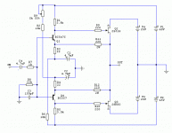
If you look for complementary design that will use both P-ch. and N-ch. VFETs, why not make it using a proven F5 topology:
In order to properly bias the VFETs we need additional rails (V1 & V2) but we can easily make them from main rails (V4, V5) by using a voltage doubler. V1, V2 need to supply only about 10ma per channel each.
R9 pot will set the DC offset at the output. R6 and R2+R9 determine the current through input BJTs (as drawn it's about 2.5mA - you can use CCS here).
I think that 1A is a nice bias for K60/J18 VFETs (at 25V Vds) so I set the values of R1 and R5 towards that goal. If you want less current (VFETs closer to AB class) just raise the value of R1, R5.
The gain is set by R11/R3 and R12/R4 ratio (20dB as drawn). C1, C2 (4700uF/6.3V) provide AC ground for input BJTs' emitters.
You can avoid additional V1, V2 rails if you use VFETs as Source Followers which would be pity, considering their unique triode properties which really come into play when they are used as voltage gain devices.
Attachments
Last edited:
Now I see that I drew C1, C2 polarities incorrectly in the post #54 schematic - they should be the other way round...
Thanks Mos57 and Juma that's an interesting schema...F5 with Sit's....wow I been planning to make a F5 before i shifted to tubes....now this got me a best idea....using vfets to a hybrid ans SS design....
Making other Vsupply is not a problem...i have a lot of trafo to use as weel as 24.5v 10A smps.
Making then as source follower will not give amplification...i want them to amplify the sound to hear what their triode properties reveal in music...
I will look on to my parts bin to see what i have to start this thing...
BTW,will this thing work even my Vfets are not of the same rank?
Yes, but first you measure your VFETs (Id vs. Vgs at Vds=25V) so you can match their working conditions (the value of R1, R5 and R2+R9, R6). The point is to make VFETs to pass the same Id so you'll have the zero DC offset at the output....BTW,will this thing work even my Vfets are not of the same rank?
It can be done in the circuit by making a R1, R5 5k trim-pots (as in original F5 circuit), but here you'll start adjustment process with a maximum value of pots and turn them slowly until you get the wanted bias and zero DC offset at the output. In this case you don't need R9 so R2, R6 can have the same value.
I guess i will consider both option as to adjust operating points.
So R1 and R5 adjusts the offset voltage and R2+R9 and R6 will do the bias current, am i right?
So R1 and R5 adjusts the offset voltage and R2+R9 and R6 will do the bias current, am i right?
Member
Joined 2006
How about modifying from this J. Hiraga Vfet amp circuit?
The Class-A Amplifier Site - Hiraga 20W Class-A
The Class-A Amplifier Site - Hiraga 20W Class-A
There's a loophole in that design by Mr. J. Hiraga as per ILIMZN, see post #25 of this thread. Maybe modifying the circuit may work. May those knowledgeable in modifying this will comment on how to make the circuit work with VFETS.
ILIMZN ,Juma and MOS57 or anybody out there may have an idea?
ILIMZN ,Juma and MOS57 or anybody out there may have an idea?
- Status
- Not open for further replies.
- Home
- Amplifiers
- Solid State
- What to do with this Sony V-FETS?