Member
Joined 2009
Paid Member
I saw the combo once before, but it was used in Class A, by Wavebourn if remember. But still, it is darn wacky and I would never have considered it until I reverse engineered a certain persons amp few years ago that also uses the Fet bjT combo (i always keep such secrets to myself). Nice to know you have found it a promising avenue too.
Last edited:
Bigun
I have used so far 3.3kR and 1kR-pot in front of the Vbe and it seems to be ok.
The most funny thing is that amp looks like made of left overs, one transistor at input, only half of the Vas and some mosfet + bjt transistors founded on the floor begind the desk 😛
I have used so far 3.3kR and 1kR-pot in front of the Vbe and it seems to be ok.
The most funny thing is that amp looks like made of left overs, one transistor at input, only half of the Vas and some mosfet + bjt transistors founded on the floor begind the desk 😛
Well I got the idea came while I was mucking around with Gareth's TGM8, grafting a pair of complementary lateral MOSFETs to his front-end in the schematic here.
Unhappy in the knowledge that I'd lose an unacceptable amount of headroom in the MOSFET version with the low rail voltages I had in mind, but not wanting to deal with the complexity of separate boosted rails, since I was working on a "Blameless" derivative that was (is) doing my head in with ever increasing complexity. It occurred to me that the action of the VAS bootstrap would help better saturate one one side but not the other.
I was on a mission of minimalism, and it also occurred to me that if I put a BJT on the other rail, I might improve headroom and clipping symmetry than with an all MOSFET output stage. A BJT needs a driver and my mind wandered back to this quasi project I'd started some weeks earlier... A quasi output stage needs at least one driver (no matter how minimalist...) so I flipped Gareth's amplifier upside-down so the bootstrap was lifting the N-MOS
I figured it would sound rubbish (even if by some miracle it actually worked!) so I'm pretty stoked to learn that it not only works, but sounds fabulous in the NAD 310, Quasimodo, etc.
Now that borys has shown the way I'm super excited and can hardly wait for my own boards to arrive!
Member
Joined 2009
Paid Member
I was thinking too that the amp looks kinda odd with different sized parts and colors and whatnot but it adds to the charm and uniqueness of it.
Christian, your brain is running fast, you have enough knowledge without being constrained by convention and it allows you to come up with nice ideas. This is a fun time and I hope, like most of us, you have a notebook to capture all your ideas over time, Leonardo style!
Christian, your brain is running fast, you have enough knowledge without being constrained by convention and it allows you to come up with nice ideas. This is a fun time and I hope, like most of us, you have a notebook to capture all your ideas over time, Leonardo style!
Ranchu32
You will be surprised I am sure!! It needs a bit of more work but this is what gives a fun and satisfaction.
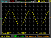
There was a mistake on my board so I have prepared V2 one. I have moved the lower emiter resistor to the colector side. The NFB I have tryed so far 47/1k --> there was too much current drawn from the nfb network so 1mF capacitor was discharged too quick, for music was ok but square wave tests failed badly, I have changed temporary NFB to 470/10k and square waves were OK.
The output bias seems to be only a small bit over compensated so as Bigun suggested the resistor network in Vbe can be lowered a bit.
The offset at the output is bit unstable (hot/cold = 200mV ).
I didn't soldered the VAS load resistor so far - try that trick later on.
So far so good.
You will be surprised I am sure!! It needs a bit of more work but this is what gives a fun and satisfaction.
There was a mistake on my board so I have prepared V2 one. I have moved the lower emiter resistor to the colector side. The NFB I have tryed so far 47/1k --> there was too much current drawn from the nfb network so 1mF capacitor was discharged too quick, for music was ok but square wave tests failed badly, I have changed temporary NFB to 470/10k and square waves were OK.
The output bias seems to be only a small bit over compensated so as Bigun suggested the resistor network in Vbe can be lowered a bit.
The offset at the output is bit unstable (hot/cold = 200mV ).
I didn't soldered the VAS load resistor so far - try that trick later on.
So far so good.
Attachments
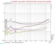
I have few more postcards. I tryed simple VAS transistor too and it seems to be ok but so far I found one diffrence to Ranchus VAS, with single transistor the THD spectrum is different threw the output amplitude range but with Ranchu's VAS the THD has very similar character threw the output amplitude range.
I have missed one detail, the input compensation transistor is different type to the input one - so I will have to change it.
Bigun
The small question - input temp compensation - set the power dissapation on the both transistors the at the same level (input and compensation transistors) ? So they will heat up the same way or set the compensation transistor a bit lower so it will take a small bit of VAS transistor temp drift ? Or just experiment 😛
Now the nfb resistor network:
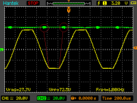
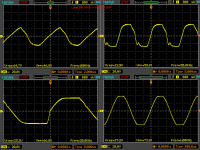
-47R-1k - the square wave's --> game over, 1mF cap is discharged completly and output looks like my 2yeares old daughter drawing 😛
-150R-3.3k - square waves are ok at 1-4kHz but at higher f looks like a drawing as above
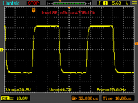
-470R-10k - i can do the square wave tests ok.
I have no decoupling caps right now on the board but please take a look at the clipping at the mosfet side rail supply, it needs some investigation.
Right now da Ranchu's time machine is driving rs125 paired with tw022wa04 monitor, time for ''the ear'' tests.
I have missed one detail, the input compensation transistor is different type to the input one - so I will have to change it.
Bigun
The small question - input temp compensation - set the power dissapation on the both transistors the at the same level (input and compensation transistors) ? So they will heat up the same way or set the compensation transistor a bit lower so it will take a small bit of VAS transistor temp drift ? Or just experiment 😛
Now the nfb resistor network:
-47R-1k - the square wave's --> game over, 1mF cap is discharged completly and output looks like my 2yeares old daughter drawing 😛
-150R-3.3k - square waves are ok at 1-4kHz but at higher f looks like a drawing as above
-470R-10k - i can do the square wave tests ok.
I have no decoupling caps right now on the board but please take a look at the clipping at the mosfet side rail supply, it needs some investigation.
Right now da Ranchu's time machine is driving rs125 paired with tw022wa04 monitor, time for ''the ear'' tests.
Attachments
-
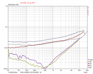
 150r-3.3kR thd 35V.jpg65.1 KB · Views: 1,224
 -
 150r-3.3kr thd 40v simple vas.jpg74.1 KB · Views: 1,213
 -
 thd 30V 47r-1kR.jpg69.3 KB · Views: 1,178
 -
 thd36v 470R-10k.jpg69 KB · Views: 1,174
 -
 20kHz.png127.5 KB · Views: 1,189
 -
 SR.png121.3 KB · Views: 306
 -
 lower clipp.png128.3 KB · Views: 291
 -
 upper clipp.png139.7 KB · Views: 295
Hi Borys
Are you able to show the results with normal sine waves? More importantly, have you been able to listen to it yet? :-D
Are you able to show the results with normal sine waves? More importantly, have you been able to listen to it yet? :-D
I will post tomorrow. Please write down what you need (what amplitude and what frequency) and I will post it tomorrow.
Yes I was listening the amp for about 16-20 hours so far. I will have to improve the wiring on my messy bench and take the thd measurements again.
Yes I was listening the amp for about 16-20 hours so far. I will have to improve the wiring on my messy bench and take the thd measurements again.
Borys,
Don't be too worried about the measurements. This type of amp does not measure very well, high levels of H2, H3 and H4. Square won't be wonderful either, although the recovery from clip is excellent. Trust your ears, however.
Congratulations on getting it laid out and built so quickly.
Hugh
Don't be too worried about the measurements. This type of amp does not measure very well, high levels of H2, H3 and H4. Square won't be wonderful either, although the recovery from clip is excellent. Trust your ears, however.
Congratulations on getting it laid out and built so quickly.
Hugh
AKSA
I will try to do as many listening test as possible, the measurements were bit worse because my wiring meas on the bench. But it is really interesting piece of amp.
I am waiting for Ranchu to get his board done and some feedback, togheter will be easier to work further.
At the moment i have soldered MJE350 in vas and as a lower driver, there can be bit sticky, slowly comming back to live after get saturated, i will solder some better trannies and compare results.
I dont mind if the amp isn't very good in measurements while it sounds right but I have to check if it is stable. The next step is to work a bit on the compensation because with capactive load the overshoot is quite big - i do not know if it is important factor but do not won't the amp to ''answer the questions asked by itself'' i mean oscillations with difficult loads.
THX
Today I have tidy up the wiring and voila:
Attachments
Last edited:
Hi Borys, Ranchu,
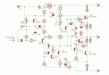
I have the latest schematic, appended.
A few points I noticed:
1. C3, lag compensation, should be about right but I would connect between emitter of Q2 and base of T3. Collector of T3 is very high impedance; it's over compensated.
2. C4, phase lead, should be 12pF.
3. T3 should be very low Cob and high beta and speed. I suggest a KSC1845.
4. C6 bootstrap works best from the output, is improves stability at high output.
5. The Vbe multiplier will generate around 5V bias. This will create almost 8 pn tempcos, and you really only need about half that. If you inject a free air 4002 diode into the emitter of Q1, increase pot R12 to 2K and use 1K8 for R13, you will get around the correct compensation as the outputs warm up.
6. I would replace D2 1N4148 by a 4002 since the smaller diode will blow at around 100mA. If Q5 is at 5A, you much be driving almost 100mA current into the base, and almost all of it comes through D2.
7. I would add a 1.5uH inductor in series with a 10R damper in the output lead.
To test the thermal behaviour, use a hair dryer on the outputs will playing!
Has AlexMM agreed to have a shot at this layout? He is the master of the audio ringside, that guy......
Nice circuit,
Hugh
Attachments
Last edited:
Borys,
I would love to join the fun, unfortunately my printed circuit boards are on a ship, somewhere between Taiwan and Australia! I anticipate it will be another week, perhaps two, before they arrive.
AKSA,
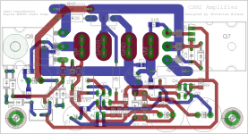
The board layout i posted at #63 is what I came up with and matches the boards currently en-route to my address. If my layout is deficient I would gratefully accept any criticisms and rectify them. I'll also send Alex MM a message and find out if he's interested in producing a version.
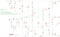
Schematic and board layout attached.
I would love to join the fun, unfortunately my printed circuit boards are on a ship, somewhere between Taiwan and Australia! I anticipate it will be another week, perhaps two, before they arrive.
AKSA,
The board layout i posted at #63 is what I came up with and matches the boards currently en-route to my address. If my layout is deficient I would gratefully accept any criticisms and rectify them. I'll also send Alex MM a message and find out if he's interested in producing a version.
Schematic and board layout attached.
Attachments
AKSA
Thanks for replay!! I will make the changes soon and try it out.
It would be superb if Leonardo DaVinci of audio pcbs AlexMM will prepare a nice tidy board.
Thanks for replay!! I will make the changes soon and try it out.
It would be superb if Leonardo DaVinci of audio pcbs AlexMM will prepare a nice tidy board.
Ranchu,
Looks terrific - at least from where I can see it!
One detail; D6 should be inserted between emitter of Q8 and the bottom of VR3. Thermally bond Q8 on the mosfet, and keep the diode in free air.
The only question will be the tempco issues with the bias current, might be a big strong, but better to reduce with increasing heat than the reverse...... this is a trick on PA amps.
You might consider fiddling R21 too. At 470K your set OLG of first and second stage is 470k/47, a tad high at 100k (100dB)!
Very nice schematic to read, well drafted. Clean drafting is much easier to understand.
Cheers,
Hugh
PS: Borys, AlexMM is better than Leonardo, he is Tintoretto....
Last edited:
Ranchu32
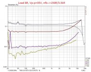
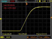
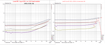
I have made some sine tests today. One test with 150R-3.3kR nfb resistors and the second test with 470R-10kR resistors.
If I will drive harder the amp with lower nfb resistors values it behaves very badly at higher frequences (take a look at the amplitude), even it is burning both fuses on the board. If I lower the nfb resistors values it it gets better. I do not know if this is some fault on my board or the impedance of the AC ground is too high. I am wondering if Bigun can give some advice here.
The 1000uF cap on my board is Panasonic FC.
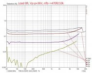
As a VAS load resistor I have used 100kR value (nfb network 470/10k), look how the harmonics spectrum is nicely dropping down, smooth threw all audio band.
I have made some sine tests today. One test with 150R-3.3kR nfb resistors and the second test with 470R-10kR resistors.
If I will drive harder the amp with lower nfb resistors values it behaves very badly at higher frequences (take a look at the amplitude), even it is burning both fuses on the board. If I lower the nfb resistors values it it gets better. I do not know if this is some fault on my board or the impedance of the AC ground is too high. I am wondering if Bigun can give some advice here.
The 1000uF cap on my board is Panasonic FC.
As a VAS load resistor I have used 100kR value (nfb network 470/10k), look how the harmonics spectrum is nicely dropping down, smooth threw all audio band.
Attachments
Last edited:
Hmm, try a 22uF cap from emitter of ground. I suspect some of this bad behaviour at HF is due to the bias system.
Hugh
Hugh
- Home
- Amplifiers
- Solid State
- Very simple quasi complimentary MOSFET amplifier