fyi - As a result of a request I made a couple of years ago, the forum now allows you to post the LTSpice file with .asc file extension so that you can share your simulation files here easily.
Thanks, I hadn't noticed that was possible tbh, but I see now that .asc are "on the list"
Thanks 🙂

I've never used Eagle, and besides, checking layouts is a very very time consuming job 🙂
Check, check and check again and make sure the critical grounds are arranged so they don't interact with anything. Make any pads as big as you can because in reality they will look small and fragile on a real board. Same for track widths.
Check, check and check again and make sure the critical grounds are arranged so they don't interact with anything. Make any pads as big as you can because in reality they will look small and fragile on a real board. Same for track widths.
Member
Joined 2009
Paid Member
Nice and compact !
I would have to think about it a bit more, but if you can forgive a bunch of nit-picks to start with ?
a few very thin traces - I don't like very thin traces and you have space to avoid them. Thin traces have higher inductance and are more easily damaged, plus the pads they connect to are less likely to the 'lift up' from a hot iron if there's plenty of copper connected to them.
some traces are rather close to through hole pads, I prefer not to push the design-rules of the board house but instead to leave more clearance than they require. For example, the ground trace going up the left side is very close to VP and could be moved to the right rather easily. There are many more examples where you can create more space between traces and through-hole pads and a couple of places where you have SMT pads close to through-hole pads that should be avoided or you'll find it hard to avoid solder bridges e.g. R16 and Q4.
I'd put a big block of copper around the QuickFit connectors used for OUT rather than rely on the connector to join the pads together and then the feedback take-off point can come from the physical centre between them.
I try to keep high current traces close together like twisted pairs so that the outbound current flows next to the return current path - reducing current loop area. I also keep high impedance nodes, like the nfb feedback point, away from high voltage swings - reducing electrostatic pick-up.
Make it easy to probe key voltages.
I have found that I end up exploring several alternative layouts before I'm happy - I might be rather too anal about it though !
Hello everyone,
Its been a while since I last posted in this thread; however, I haven't forgotten about it, nor have I been sitting on my hands! Lately I've been spending far too much time playing with Eagle, time I could spend under the house building amps ;-)
In the last few days I've been toying with Bigun's TGM8 project, in Eagle, and grafted a lateral FET output stage to the front-end.
Consequently, I decided revisit this quasi-complimentary design, dispensing with the LTP input stage and substituting it for a singleton transistor with Bigun's novel biasing scheme.
It occurred to me that it may be possible to develop a type of "hybrid" quasi output stage, consisting of a vertical MOSFET for the positive swing and a BJT compound pair on the negative rail. I have no idea whether this will by some miracle actually work, and if so sound good, but the idea appeals to me.
I've inverted Bigun's input stage so that the VAS bootstrap sits on the positive rail, providing a little extra drive voltage into the MOSFET to theoretically improve clipping symmetry. The VAS runs relatively "hot" to help overcome the MOSFET's gate capacitance. In Bigun's thread he suggested a compound VAS arrangement to increase the impedance seen by the input transistor and I made it so...
Today, I spent some time experimenting with the compensation on a spare TGM8 board. Using my crude oscillation detector (pocket AM transistor radio) and my ears I resolved that it is stable with the smallest NP0 I had on hand - a 12p ceramic. With no compensation I could detect (relatively benign) oscillation. Experimentation with the two-pole scheme brought no sonic benefit (to my ears) and so I've omitted it in this schematic. FetZilla is specified with a 15p silvered mica and that seems a reasonable starting point.
Look forward to your comments and improvements.
Attachments

Hi Ranchu!
NAD made a small amp with a similar output stage. 301 or 310 was the name I think.
Thorsten
NAD made a small amp with a similar output stage. 301 or 310 was the name I think.
Thorsten
Thank you Thorsten, your "NAD 310" reference led me to the schematic, a single rail design with a single NMOS and "complimentary" emitter-follower PNP BJT's.
My search also turned up your 4 year old thread discussing this same amplifier:
http://www.diyaudio.com/forums/soli...l-kind-thd-mosfet-bjt-new-me.html#post2140251
My search also turned up your 4 year old thread discussing this same amplifier:
http://www.diyaudio.com/forums/soli...l-kind-thd-mosfet-bjt-new-me.html#post2140251
Christian,
This will sound very good, but have high THD, particularly H2 and H4.
This output stage has been built by a UK company, I think Cambridge.
Nothing is new, but few are recognised that are outstanding......
Have a look at Herve Delacraz' Dartzeel. It is wonderful!
Nice pcb, you learn damn quick.
Hugh
This will sound very good, but have high THD, particularly H2 and H4.
This output stage has been built by a UK company, I think Cambridge.
Nothing is new, but few are recognised that are outstanding......
Have a look at Herve Delacraz' Dartzeel. It is wonderful!
Nice pcb, you learn damn quick.
Hugh
Last edited:
NAD also produced the L40 receiver around 1999. Almost identical to NAD310, it paired a BUK555 with a common 2SA817 BJT in a very economical and simple output stage - singleton input stage for around 20W/8R. Logic-level Mosfets with generous Rds for audio use, like the extinct BUK 555 are rare now, unfortunately. NAD L40 Manual - Compact Disc Receiver - HiFi Engine
http://www.hifiengine.com/manual_library/nad/310.shtml
http://www.hifiengine.com/manual_library/nad/310.shtml
Last edited:
Member
Joined 2009
Paid Member
I know Hugh is quite familiar with this output stage (and many others) and if he says it will sound good I would bet money on it 🙂
Thanks Hugh, I read about your loss and you have my condolences. The Dartzeel appears extremely high-end from the exterior but the component count is very small on the schematic.
Ian, thanks for that reference, you've given me some more reading material to ponder.
I will keep plugging away and update when I think I have something interesting to add...
Ian, thanks for that reference, you've given me some more reading material to ponder.
I will keep plugging away and update when I think I have something interesting to add...
If you are looking at the Nad 310 then don't overlook another of its secrets. Look at the output and R255/C225 and R256/C226.
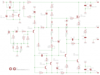
Update
Mooly, WOW... there is intentional cross-conduction between the two channels 😱
The schematic I posted on the last page seems to have generated a small amount of interest. A very clever, helpful, Australian designer has been in contact with me to discuss some of the finer details (and for the avoidance of doubt it is not Hugh, although he certainly fits all those critera!).
As is often the case, these suggestions have led to further research and new ideas, but these will wait for another project. I want to keep this "very simple" and I still think it meets that criterion.
I'm still working on the board layout - obsessively - I want this to better the last.
In the meantime here's the latest schematic. I got the idea for R22 from some of OStripper's designs ("VAS abuse - his words 😀). Seems to increase H2 and slightly lower H1.
Attachments
Member
Joined 2009
Paid Member
Looking good, I like this approach !
(R22 - is a good idea, nested feedback, you have it in TGM8 too)
(R22 - is a good idea, nested feedback, you have it in TGM8 too)
Mooly, WOW... there is intentional cross-conduction between the two channels 😱
Yes 🙂 Another of its little "subjective performance secrets"
Looking good, I like this approach !
(R22 - is a good idea, nested feedback, you have it in TGM8 too)
I'm taking a break from my Blameless MkII. The component count has skyrocketed (the current design is more complex than the last schematic I posted...) and its making my head hurt.
Having some fun with this one by trying to optimise - instead of minimise - the THD.
The gentleman I spoke of earlier is Richard McDonald, an Australian amplifier designer. Richard has kindly shared some information which "does not compute" with what I have learnt from reading Self, Cordell et al. I'm still trying to process it.
I've not heard Richard's line personally and first became aware of them around a year ago when I bought a pair of floorstanders from Adelaide Speakers (Quasimodo Stereo Amplifiers). Edward, the loudspeaker builder behind the brand loves to chat and was very complimentary of Richard's product. I'm extremely happy with my speakers so I'm inclined to trust his judgement in audio matters generally.
It really is a small world (here in Australia anyhow!).
Christian,
Richard and I are friends and have been collaborating with amp design for 15 years.......
Lovely guy, very active, and with a wonderful ear too. He and I created the AKSA in 2000.
Hugh
Richard and I are friends and have been collaborating with amp design for 15 years.......
Lovely guy, very active, and with a wonderful ear too. He and I created the AKSA in 2000.
Hugh
Member
Joined 2009
Paid Member
It seems to me that Hugh and Richard are still keeping close - there is something in the air in Australia that keeps lots of good ideas flowing.
Last edited:
I'd add a resistor (e.g. 82R) in the power rails with cap to ground, to isolate the front end from the power output stage.
This will also help with hum with little or no signal.
I did this with my mosfet amp and it is dead silent with no signal.
there is something in the air in Australia that keeps lots of good ideas flowing
It's in the air everywhere, Gareth, OCD in modern times, 'nerdiness' back in the eighties.
Most of us in the SS forum are afflicted with this wondrous affliction. I find amp design the most intellectual pursuit I know, certainly it suits me.
Ciao,
Hugh
- Home
- Amplifiers
- Solid State
- Very simple quasi complimentary MOSFET amplifier