The FPGA connectors are a real pain. Even when they looked soldered down, I would get no continuity from the actual connector pin and it's destination. In my initial checks, I had accidentally concluded there was continuity to the correct destination because I was touching the pad.
Yes, the FPGA connectors are a real pain. I removed the FPGA and reflowed the pins of J5 but to be honest they looked worse once I was finished than they did at the start. What I did do when re-installing the FPGA was to not use the plastic standoffs. I know right! They helped me wreck the first pcb in my impatience so why would I use them again? Well, everything to date that I have made that fits into my playback is point-to-point (aka ratsnest) wiring which is much more "stable" than a large flexible pcb that feels cumbersome in comparison. Anyway, those little standoffs were a way to 'firm up' things a little and because I did not want the FPGA dropping off if the pcb was flexed a little hard or sagged over the long-term. What I think was happening was the standoffs were not quite exactly the correct length (7mm apparently) and the FPGA may or may not have been sitting a little prone in its sockets and the 3.3V connection may have been compromised.
The reason I say this is because I reseated the FPGA without any soldering of J5 and managed to get 3.03V for P9.19 and P9,20, which previously was 0.033V. Not quite 3.3V but better, and over time this voltage dropped a little, perhaps as the connections heated up a little. So I pulled off the FPGA a second time and touched up the J5 pins and then replaced the FPGA without the standoffs...and it fired straight up...85A2 shining like a dull orange sun.
Phwew.
Now to see if it actually works and can make some music.
Last edited:
Marcel,
Thank you for all your help thus far.
Before getting in and debugging the JLSounds I2SoverUSB3 card, is there a way to verify that the dac is working properly by some other means? It is probably pointless debugging the USB card if I am not sure the dac is working. Have not bothered yet with inputs other than USB.
The clock trimmed just fine. Plugged into my preamp I have audible noise which measures about 0.2mVAC for left channel and a bit more on the right (have not tried to trim the output tubes yet). That noise will have to come down quite a bit but is a job for later.
Anthony
Do you hear the output relays switching when you change the sigma-delta mode or the filter setting?
Do you get sound when you connect an S/PDIF source?
You can to some extent check the USB card without the valve DAC when you have an oscilloscope or a resistor and two capacitors. With an oscilloscope you can just check if you get a bit clock, word clock and data, without an oscilloscope you could use it in native DSD mode and check with a makeshift low-pass filter if you get any audio.
If you have two generators at your disposal that can produce 0 to 3.3 V square waves, you can set the I2S interface to raw (native) DSD mode, apply a square wave of about 2.8 MHz to the bit clock input and an audio frequency square wave to the data and word clock inputs. The clipping light should then turn on and you should hear a loud sound at the frequency of the audio square wave.
No, there is no sound from the output relays when changing sdm or filter settings. Have never heard them make a noise. Perhaps I need to track down this issue first.
Have just been rummaging around and found something that may be able to be used as a SPDIF source on one of the HDMI to I2S converters recently purchased. Will hopefully be able to HDMI from the Pioneer UDP to the converter which will output coaxial (which I assume is SPDIF).
Nothing special required for SPDIF input to the ValveDac? Just a RCA or BNC connector with two wires to a couple of pins in P7?
Have a 2 channel analogue generator that will do up to 10Vrms. Also have an analogue scope. The absence of relay noise points to something to first investigate.
Do you measure 3.3 V to ground on all open switch contacts (and 0 V when the switch is closed)?
The JLSounds board has an SPDIF output?
Looking at the documentation, it appears to be a logic level output meant to drive a Toslink transmitter rather than a real 75 ohm S/PDIF output.
No, there is no sound from the output relays when changing sdm or filter settings. Have never heard them make a noise. Perhaps I need to track down this issue first.
Indeed. Testing whether you see 3.3 V on all open switches and testing whether the 27 MHz clock ever reaches the FPGA module are two things you can try. Do you see a 27 MHz square wave between any terminal of R124 and ground?
Nothing special required for SPDIF input to the ValveDac? Just a RCA or BNC connector with two wires to a couple of pins in P7?
Yes, pins P7.15 and P7.13, or P7.11 and P7.9, or P7.7 and P7.5. There has to be a 75 ohm termination resistor on the valve DAC board for the input you use. It has its advantages to have an S/PDIF transformer on either the transmitting or the receiving side (can help to avoid ground loops and suppress common mode interference), but it is not needed at all for a basic functional check.
Have a 2 channel analogue generator that will do up to 10Vrms. Also have an analogue scope. The absence of relay noise points to something to first investigate.
Can you set the offset of the generator so its outputs swing between 0 and 3.3 V with no load? (I write "with no load" because I once subjected a chip to twice the intended voltage level, because the generator displayed the characteristically terminated voltage and there was no such termination.)
Last edited:
Looking at the documentation, it appears to be a logic level output meant to drive a Toslink transmitter rather than a real 75 ohm S/PDIF output.
Ah, OK. I haven't looked closely at the V3 board but my V2 boards have an SPDIF coax output.
What I read in the documentation applies to H3 pin 9, but apparently there is also an H2 that is marked "S/PDIF" on a drawing of the PCB. Is that the 75 ohm S/PDIF output?
All switch contacts apart from one behave as expected: SW2 position 4 for the halfband filter. The contact makes ground just fine but has no 3.3V when the other filters are selected with the switch. Other filter selections behave as designed, just not the halfband one.
nautibuoy, I just had a look and SPDIF can be taken from the JLSounds board. Thanks for the heads-up...I'll set it up.
nautibuoy, I just had a look and SPDIF can be taken from the JLSounds board. Thanks for the heads-up...I'll set it up.
[snip]...and testing whether the 27 MHz clock ever reaches the FPGA module are two things you can try. Do you see a 27 MHz square wave between any terminal of R124 and ground?
Will have to pull out the oscilloscope from storage to see if I am capable of measuring such a thing. Would like to give it a go. I have no electronics background so may not yield a suitable result.
With a scope bandwidth of 10 MHz or less, you will probably hardly see anything. With a 20 MHz scope, you will probably see something that looks more like a sine than like a square wave. With a bandwidth of 80 MHz or above, it will look more like a square wave than like a sine. Depending on the type of probe and how you connect the ground lead, you can then also get ringing at some very high frequency.
In any case, when you see a DC level that's neither very close to 3.3 V nor very close to zero with something wiggling at a 27 MHz rate, then you know it works.
In any case, when you see a DC level that's neither very close to 3.3 V nor very close to zero with something wiggling at a 27 MHz rate, then you know it works.
I2SoverUSB has two sets of output pins marked SPDIF. There is a SPDIF pin on H3, and another SPDIF and ground, 2-pin header at one end of H3. Haven't checked either one for source impedance. The I2S output pins are source terminated for nominally 50-ohm lines.
Also, in Windows I have sometimes seen a separate sound device which is called something like I2SoverUSB_SPDIF, so routing audio there may require sending signal to the correct device driver.
Also, in Windows I have sometimes seen a separate sound device which is called something like I2SoverUSB_SPDIF, so routing audio there may require sending signal to the correct device driver.
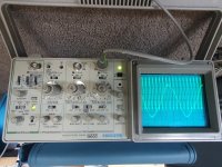
Given my amateur status, I thought some context to my measurements should be included (see attached photos).
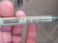
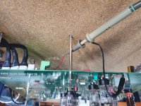
Scope is Tek 2225 50MHz. Using a P6119 probe at 1x set between the ground side of R52 and a wire solder to one end of R124. One of the images shows the traces at 0.2V/div and 0.05uS/div (magnified trace at 10x horizontal).
Look to me like the frequency is circa 36MHz and voltage is roughly 1Vpp. Note that I did this with a 10x probe (P6103) which resulted in the same frequency and Vpp.
Clock is definitely 27MHz...says so on the top of the case.
Attachments
- Home
- Source & Line
- Digital Line Level
- Valve DAC from Linear Audio volume 13