I measured the current with my BM235. I got almost exactly 3A for the 6.3v, measured at my regulator output. For -300v, I measured at the positive output of my Maida and it was 67mA.
The 75 mA I put in the opening post is a somewhat conservative calculated value, so that fits well with your measured 67 mA. My 2.7 A is the sum of the datasheet values of the valve heater currents (neglecting the 31.5 mA through the two 100 ohm resistors), but some E88CCs draw a bit more heater current than others. I'll also put your measured values in the opening post.
I had to put things on pause until parts for a beefier 6.3V supply come in. The diodes were cooking, so I'm mounting them off-board onto a big heatsink.
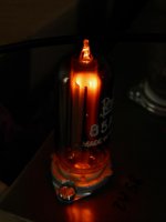
Normally you would see the cathode of the 85A2 light up, that is, the rod at the centre. With reversed polarity, the anode would light up, that is, the cylinder around the cathode. It may be difficult to see due to the molybdenum gettering, though.
For the record, I mixed up the anode and the cathode. The cylinder is the cathode and the rod is the anode, so it's the cylinder that normally lights up. Attached are a picture from G. F. Weston, Cold cathode glow discharge tubes and a home-made photo of a Pope 85A2 with relatively thin gettering.
Attachments

Originally, when I drew the schematic and designed the PCB, P9 was an extension connector with no specific purpose. Later randytsuch asked me to add an I2S input and I used P9 for that. It is explained on the downloads section of the Linear Audio website, "Design data package for Marcel van de Gevel's Valve DAC from Vol 13":
P9 pin 1: sel4192in, 0 selects the I2S (or raw DSD) input, 1 selects the DIX4192 S/PDIF interface. Debounced input with internal pull-up that can be connected to a fifth contact of the source selection switch.
P9 pin 3: mutei2sin, 1 mutes the sound when it comes from the I2S input.
P9 pin 5: datai2sin, I2S audio data input or raw DSD left audio data input.
P9 pin 7: deemni2sin, low level activates 50 us/15 us de-emphasis when the I2S input is active.
P9 pin 9: bcki2sin, bit clock for the I2S or raw DSD input.
P9 pin 11: lrcki2sin, word clock for the I2S input or right channel raw DSD data.
P9 pin 13: dsd64_128, must be 0 for DSD64 and 1 for DSD128 when the raw DSD interface is used.
P9 pin 15: dsdon, must be 0 for PCM or DoP, 1 for raw DSD.
P9 pins 2, 4, 6, 8, 10, 12, 14, 16: ground
P9 pins 17, 18, 19, 20: 3.3 V supply pins, see the schematic.
All inputs have internal pull-ups except dsdon and dsd64_128, which have internal pull-downs. The extension connector can be left unconnected when the I2S input isn't needed. The logic high level is nominally 3.3 V.
You need version 2.1 of the configuration file for the I2S input to work.
Marcel,
I have a little bit of time to get this dac operational and am having trouble with the I2S wiring from the JLSounds I2SoverUSB3 board (see attached manual).
My interpretation is as follows:
P9.1 <---- ??
P9.2 <---- ??
P9.3 <---- JL H3.20
P9.4 <---- ??
P9.5 <---- JL H3.13
P9.6 <---- JL H3.14
P9.7 <---- ??
P9.8 <---- ??
P9.9 <---- JL H3.11
P9.10 <---- JL H3.12
P9.11 <---- JL H3.15
P9.12 <---- JL H3.16
P9.13 <---- ??
P9.14 <---- ??
P9.15 <---- JL H1.8
P9.16 <---- JL H1.10
P9.17/18/19/20 no connection
Big holes in my knowledge right there.
Anthony
Attachments
The manual isn't entirely clear to me either, but you could try this:
P9.1 <---- fifth contact on the source selection switch if you also want to use the DIX4192 inputs, can be connected straight to P9.2 when you only need the I2S/raw DSD input
P9.2 <----
P9.3 <---- JL H3.20
P9.4 <---- JL H3.19
P9.5 <---- JL H3.13
P9.6 <---- JL H3.14
P9.7 <---- leave open, or connect a switch between P9.7 and P9.8 (*)
P9.8 <---- leave open, or connect a switch between P9.7 and P9.8 (*)
P9.9 <---- JL H3.11
P9.10 <---- JL H3.12
P9.11 <---- JL H3.15
P9.12 <---- JL H3.16
P9.13 <---- JL H1.5
P9.14 <---- JL H1.2
P9.15 <---- JL H1.8
P9.16 <---- JL H1.10
P9.17/18/19/20 no connection
(*) With such a switch you could manually activate the de-emphasis if you ever use the I2S interface to play rips of CDs with pre-emphasis. Those would typically be very old CDs, as using pre-emphasis/de-emphasis on CDs very soon went out of fashion.
It's a pity that the connections straight to H1 are needed, as those mess up the isolation feature of the USB interface board. If you don't want that, you will have to add two optocouplers and a few resistors or one optocoupler, some resistors and an inverter.
By the way, the only DSD formats that the original valve DAC supports are 44.1 kHz-based DSD64 and DSD128, so 2.8224 MHz and 5.6448 MHz sample rate. Other DSD formats will probably result in loud noise.
This applies with the raw (native) DSD input, as using DoP, it only supports 44.1 kHz-based DSD64 (2.8224 MHz).
For the record, I mixed up the anode and the cathode. The cylinder is the cathode and the rod is the anode, so it's the cylinder that normally lights up. Attached are a picture from G. F. Weston, Cold cathode glow discharge tubes and a home-made photo of a Pope 85A2 with relatively thin gettering.
Beautiful view, fantastic job ...
Verilog + tube = 🙂
T
It's a pity that the connections straight to H1 are needed, as those mess up the isolation feature of the USB interface board. If you don't want that, you will have to add two optocouplers and a few resistors or one optocoupler, some resistors and an inverter.
Thanks Marcel, I'll give that a try. At this stage I just want to get something playing so will not bother with anything from the JLSound H1. My understanding is that the ValveDac wants to see 0V on P9.15 for PCM which also equates to all of the JL H1 wires being disconnected...which is easy to do.
We have ignition...sort of.
All valves light up apart from the 85A2. Have three green lights on the FGPA (difficult to see under there) but 0v from anode to cathode on the 85A2. Will try to follow the voltages in the supplies to see if anything is astray. -292V across C126.
All valves light up apart from the 85A2. Have three green lights on the FGPA (difficult to see under there) but 0v from anode to cathode on the 85A2. Will try to follow the voltages in the supplies to see if anything is astray. -292V across C126.
Can you check the voltages in the circuit that drives the 85A2 - the voltages you can access without shorting anything, that is? If everything were OK, you should get something like this, all voltages with respect to ground:
+3V3: about 3.3 V
nswitch85A2: first 3.3 V and then 0 V, after a second or two
collector Q8: first somewhere between -300 V and -200 V, and then +2.5 V
collector Q10: 5 V when the 85A2 is off, 0.2 V when it is on
ignited85A2: 0 V when the 85A2 is off and 3.1 V when it is on
+3V3: about 3.3 V
nswitch85A2: first 3.3 V and then 0 V, after a second or two
collector Q8: first somewhere between -300 V and -200 V, and then +2.5 V
collector Q10: 5 V when the 85A2 is off, 0.2 V when it is on
ignited85A2: 0 V when the 85A2 is off and 3.1 V when it is on
-300V, -137V, -132V all good along with 5V from L4940V5. 1.8V from the LM317.
Not sure where I should try to find 3.3V...assume it is made on the FPGA board.
Not sure where I should try to find 3.3V...assume it is made on the FPGA board.
Can you check the voltages in the circuit that drives the 85A2 - the voltages you can access without shorting anything, that is? If everything were OK, you should get something like this, all voltages with respect to ground:
+3V3: about 3.3 V
nswitch85A2: first 3.3 V and then 0 V, after a second or two
collector Q8: first somewhere between -300 V and -200 V, and then +2.5 V
collector Q10: 5 V when the 85A2 is off, 0.2 V when it is on
ignited85A2: 0 V when the 85A2 is off and 3.1 V when it is on
+3V3 is about 0.033V (D6 - R125). Checked P9.19 - P9.20 and get 0V, so it looks like no 3.3V is being sent out from the FPGA.
nswitch85A2 is 0.033V.
Collector Q8 -200V
Collector Q10 4.972V
ignited85A2 0.031V
Last edited:
That's good news, then it probably isn't a short or an early failure of the FPGA module. Just to double-check, with everything powered down, do you measure a very low resistance (say < 5 ohm) between +3V3 and ground?
Assuming you don't:
Can you check if J5 pins 35 and 36 are soldered properly? J5 pins 35 and 36 are supposed to conduct the 3.3 V from the FPGA module to the +3V3 net. What happens when you short P9.17, P9.18, P9.19 and P9.20? That would provide an alternative path from the 3.3 V to the +3V3 net.
Assuming you don't:
Can you check if J5 pins 35 and 36 are soldered properly? J5 pins 35 and 36 are supposed to conduct the 3.3 V from the FPGA module to the +3V3 net. What happens when you short P9.17, P9.18, P9.19 and P9.20? That would provide an alternative path from the 3.3 V to the +3V3 net.
Tried +3.3V at a few spots and all resistances were high with nothing even close to 5R.
The FPGA pins seem to be soldered well enough and I have continuity between C87 and J5.35. I'll pluck up the courage to remove the FPGA in the morning and reflow J5. When shorted between P9.18 and P9.20 the 85A2 instantly lights up which is certainly promising.
The FPGA pins seem to be soldered well enough and I have continuity between C87 and J5.35. I'll pluck up the courage to remove the FPGA in the morning and reflow J5. When shorted between P9.18 and P9.20 the 85A2 instantly lights up which is certainly promising.
- Home
- Source & Line
- Digital Line Level
- Valve DAC from Linear Audio volume 13