USSA-5B birth pains – and smoke!
Damn. I triple checked everything. Convinced that I did everything correct. All went well up to step 8.17.1 – Adjust output Mosfet current close to intended final bias
As soon as I connected V+ and V- and GND to the PSU (+/- 26V) there was a high pitch sound and then R15 and R16 started smoking before any measurements could be taken. I immediately switched off the power. Help. What could be wrong here?
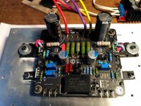
The boards are stuffed for the 5B build, using Sanken Darlingtons on input and Toshiba (2SA1943 and 2SC5200) bjts on output.
R15 and R16 are 0.22 ohm 3W, and on the photo it can be seen that they have burnt.
The only mistake that I am aware of is that P1 is fitted with the wrong orientation, but I hope this is not an issue.
Damn. I triple checked everything. Convinced that I did everything correct. All went well up to step 8.17.1 – Adjust output Mosfet current close to intended final bias
As soon as I connected V+ and V- and GND to the PSU (+/- 26V) there was a high pitch sound and then R15 and R16 started smoking before any measurements could be taken. I immediately switched off the power. Help. What could be wrong here?
The boards are stuffed for the 5B build, using Sanken Darlingtons on input and Toshiba (2SA1943 and 2SC5200) bjts on output.
R15 and R16 are 0.22 ohm 3W, and on the photo it can be seen that they have burnt.
The only mistake that I am aware of is that P1 is fitted with the wrong orientation, but I hope this is not an issue.
Attachments
First off, do you have a simple bulb limiter or Variac for startup?
Always power a new project with something to limit current.
Always power a new project with something to limit current.

Damn. I triple checked everything. Convinced that I did everything correct. All went well up to step 8.17.1 – Adjust output Mosfet current close to intended final bias
As soon as I connected V+ and V- and GND to the PSU (+/- 26V) there was a high pitch sound and then R15 and R16 started smoking before any measurements could be taken. I immediately switched off the power. Help. What could be wrong here?
The boards are stuffed for the 5B build, using Sanken Darlingtons on input and Toshiba (2SA1943 and 2SC5200) bjts on output.
R15 and R16 are 0.22 ohm 3W, and on the photo it can be seen that they have burnt.
The only mistake that I am aware of is that P1 is fitted with the wrong orientation, but I hope this is not an issue.
I tryed to convert my USSA5 to USSA5B. Smillar case happen to me but in my case the leg of mosfets was wrong. I saw the smoke 🙁 Now i am waiting for 5.2. New journey 😀
Hi Twocents
Section 8.17.1 is for mosfet output thus not applicable for bjt output.
USSA version 5B adjustments are sections 20.1.3 and up.
I do not see PGND (power ground return) connected in your picture….
P1 orientation has no effect if you adjust the voltage correctly.
For possible repair:
1) check R27 if not open or high value ( if you forgot to connect PGND)
2) replace R15 and R16
3 check your bjt output that they are not short circuit
4) readjust using section 20.1.3 of the manual
Good luck
Fab
Hi potstip
Version 5.2 is ready, work fine and sound fine too (to my ears). if you want I can add the instructions to the build manual.
Version 3.2B is also ready, work fine and sound fine. H2 adjustment is a bit more difficult though.
Fab
Version 5.2 is ready, work fine and sound fine too (to my ears). if you want I can add the instructions to the build manual.
Version 3.2B is also ready, work fine and sound fine. H2 adjustment is a bit more difficult though.
Fab
Last edited:
First off, do you have a simple bulb limiter or Variac for startup?

Hey potstip – hope you have better luck with your new 5.2 journey. For me it was deja vu. I blew up (in a more spectacular way) my TDA7293 amp a few months ago. I seem to have a streak of bad luck currently.I tryed to convert my USSA5 to USSA5B. Smillar case happen to me but in my case the leg of mosfets was wrong. I saw the smoke 🙁 Now i am waiting for 5.2. New journey 😀
Hi Fab,
Thanks - I can do with some good luck.
Guilty as charged! I did NOT connect PGND. I have a temporary PSU setup for bench testing and did not bother to connect PGND. Could this be the only reason for the smoke?
1) R27 (2.2 ohm 1% 0.5W metal film) is mounted indeed. All BOM components are mounted.
2) Hopefully only R15 and R16 needs to be replaced. That should be easy enough.
3) Yes, I checked bjt outputs for short circuit before power up.
4) Thanks, I seem to have combined the 5.1 and 5B sections of the manual.
Will report back soon.
Hi Twocents
For clarification,
1) I mean ensure R27 is not failed and still measure its 2.2 ohms value. Because if it has been subjected to the overall bias current ( missing PGND) then it might now be failed. You need to measure it.
3) I mean after , now.
If you have followed a wrong section of manual and over biased the output then it explains the failure. Also, having R27 burnt -if it is - makes portion of the amp floating and can give unpredictable results thus can provide failure too.
Fab
Last edited:
I am finalizing the gathering of parts for my build.
Wondering if shielded cable is recommend for the hookup between the RCA input jacks and the input on the USSA-5 board? If so? I am looking for cable available by the foot. I saw several single conductor shielded instrument cables are available. Would these be suitable?
Canare GS-6 Guitar/Instrument Cable Per Foot - Black
Canare GS-4 Guitar / Keyboard / instrument Cable by the Foot - Black
Also found this offering by VH Audio:
https://www.vhaudio.com/images/pulsar-cu-occ.jpg
Audio cables, parts, and tweaks for audiophiles - VH Audio
https://www.vhaudio.com/images/pulsar-cu-occ.jpg
Audio cables, parts, and tweaks for audiophiles - VH Audio
Hookup between input and board
Hi tmas
On my side I simply buy a 3 or 6 feet RCA interconnect cable well shielded and remove the RCA connectors at each end. I can do several amps or preamps or else with one cable.
Fab
Hi tmas
On my side I simply buy a 3 or 6 feet RCA interconnect cable well shielded and remove the RCA connectors at each end. I can do several amps or preamps or else with one cable.
Fab
Last edited:
Thanks FAB!
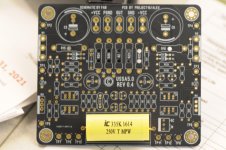
For the 3.3uf input cap I am going to try these Polypropylene units from Cornell Dubilier/Illinois Capacitor. They have a good reputation among the DIY tube community for good sound at a reasonable price. They will fit good on the USSA-5 board. The specs. look good on paper.
https://www.mouser.com/ProductDetail/Cornell-Dubilier-CDE/335MPW250K?qs=3tP%2BN51vMXeWx7ASCdq7/g==
Agreed except the 160V version is not stocked at Mouser or anywhere else I could find in the US. Hopefully I can squeeze the 250V version on the board? It looks pretty close.
Hi Fab,For possible repair:
1) check R27 if not open or high value ( if you forgot to connect PGND)
2) replace R15 and R16
3 check your bjt output that they are not short circuit
4) readjust using section 20.1.3 of the manual
For clarification,
1) I mean ensure R27 is not failed and still measure its 2.2 ohms value. Because if it has been subjected to the overall bias current ( missing PGND) then it might now be failed. You need to measure it.
3) I mean after , now.
The initial smoke was R15 and R16 getting too hot. So, there must be a huge bias current through these resistors. I measured R15 (0.22) , R16 (0.22) and R27 (2.2) and they are still good and measure their correct values.
But, I simply cannot get the bias between 1 or 1.3 A. The voltage measured between TP1/TP2 is somewhere between 2V and 3V, depending on P3. I need to work fast since the resistors get red hot. I need to try and dial the voltage down to about 300mV max. I have checked and P3 is definitely a 1k trimpot.
I really don’t know what to do or check anymore. 😕
Any ideas?
Hi Twocents
If you follow the manual section 20.1.3.4 :
2 or 3V is ten times the required value!
« Adjust final output bias current to desired value [1 – 1.3]A (200mV to 260mV with 0.2 Ohms) using P3 and
P4;… »
If you cannot get this voltage the maybe your jfet idss is unusually very high so you can increase R9/10 value to 1K ohms instead of 330 ohms.
Ensure to use both P3 and P4 to minimiz DC offset at output.
Fab
Last edited:
Twocents,
First, you should not be in the situation where you are working fast.
Build a bulb limiter and use a high wattage bulb.

Do that first and don’t do any more full voltage power ups until then. Once you have the limiter in line with the boards, then see if you can adjust final bias down to nearly 0 mV. It won’t be zero, but it will be close. Once you have established that you can get it to close to zero let us know. Then we can proceed.
First, you should not be in the situation where you are working fast.
Build a bulb limiter and use a high wattage bulb.
Do that first and don’t do any more full voltage power ups until then. Once you have the limiter in line with the boards, then see if you can adjust final bias down to nearly 0 mV. It won’t be zero, but it will be close. Once you have established that you can get it to close to zero let us know. Then we can proceed.
Hi Twocents
Thinking more about it, if you followed the manual (section 20.1.3.1 and 20.1.3,2) then it means that your Jfet current sources values were correct. Thus, please report your steps results (either « ok « or the value) here :
20.1.3 Adjustment differences
20.1.3.1 Section 8.7 Current Source adjustment
Connect V+ and V- and both PGND and GND to power supply (from 15Vdc to 30Vdc).
Connect TP10 and TP11 to Ground terminal.
Adjust P3 for about 29mV (temporary value) between TP9 and TP10.
Adjust P4 for about 29mV (temporary value) between TP11 and TP12.
20.1.3.2 Section 8.8.5 Adjust current in input stage
Connect V+ and V- and Both PGND and GND to power supply (from 15Vdc to 30Vdc).
Adjust P3 to obtain 180mV (temporary value of 900ma) bias between TP1/TP2.
Adjust P4 to obtain 180mV (temporary value of 900ma) bias between TP3/TP4.
-Report voltage between TP9 and TP10. :_________
- Report voltage between TP11 and TP12.:______
20.1.3.3 Section 8.18 Driver transistors bias adjustment
With about 180mV (900ma) bias between TP1/TP2 or TP3/TP4. Positive side:
Measure Vbe between TP5 and TP1: _______
IQ5pre = Vbe/ 20 Ohms = __________
If the IQ5pre value is not within [40-45] ma then R13 = Vbe / 42ma.
Negative side:
Measure Vbe between TP6 and TP3: _______
IQ6pre = Vbe/ 20 Ohms = __________
If the IQ6pre value is not within [40-45] ma then R14 = Vbe / 42ma.
Note: the final bias for output transistor is expected to be in the range of [1 – 1.3]A thus giving about 45mA as driver current.
20.1.3.4 Section 9 Test assembled board (no load)
With no load on amplifier output (or load higher than 10K Ohms):
Output dc offset are adjusted using P1 only;
Install the meter probe leads between TP1 and TP2(or TP3 and TP4);
Install another meter probes set between Output and Ground;
Turn P1 to center DC offset to < 5mV while monitoring voltage between Output and Ground;
Adjust final output bias current to desired value [1 – 1.3]A (200mV to 260mV with 0.2 Ohms) using P3 and
P4;
I have put in bold instructions so you always connect both grounds so no issue can arise from one missing ground.
If you had succeeded at step 20.1.3.2 to obtain 180mv there is no reason why you cannot get 200 or 260mv across R15 or R16 at steps 20.1.3.4….
Also, ensure you really have 0.2 ohms for R15/16 and not 0.02 ohms.
Ensure Q7 and Q8 are in the right position.
Also I cannot see if R4 is installed from your picture since you seem to have 2 xC1 caps installed.
Fab
Last edited:
- Home
- Amplifiers
- Solid State
- USSA-5 Build with Review