What was wrong with the buffer to begin with?
I don't know it sounds great to me, just that some here said it wasn't the best design they've seen, but then how can that be seen without all the missing bits that are not shown on the simplifed diagram.
Ho! and BTW the dc offset direct coupled all the way is only a nice stable 10mV at pin 6, I could null this out with your dac offset nulling circuit that you gave me because that's adjusted for zero at TZ, and I figure it's better to have zero there than at pin 6.
Cheers George
From studying the datasheet - the OL output impedance being 15R, the buffer's output quiescent is probably around 1mA. You could experiment with adding a current source (try to both rails) drawing say 4mA (an LM317L would work) to bias one or other of the output transistors into classA. Be sure to feed the LM317L from a very clean power supply though.
Doh, you guys just missed my previous post, go back a page. The buffer adds more distortion but as noted it doesn't sound too bad.
No, I read it. I don't consider full scale distortion to be a significant contributor to SQ. Pedja quotes the figure at 2VRMS, it would have been much more interesting to learn of the 50mVRMS figure.
Pedja is asked:
"Talking more about IV conversion I note that you did some tests previously with AD844 that found some poor distortion performance in the output stage of the 844 and I wondered was this test with feedback to the negative input terminal or open loop?"
And says:
"Once I actually posted AD844 performances both with and without feedback... Without feedback and with inverting input loaded by TDA1541A output current and impedance, a THD is at about or a bit above 0.1% (this includes both AD844 current mirrors and its output buffer, and each of these two stage are contributing about the same to this figure). With feedback it performs so good as good opamp does."
CG describes the issue:
"The AD844 is a special case. It's a current feedback type amplifier. The transimpedance node is connected to a pin on the package, which allows the part to be used open loop (actually, as the AD797 can be) if you want to run it that way. There may be good reasons to do so... Thank Barrie Gilbert for following Wyn Palmer's lead on making this pin available. (Wyn was a serious DIY audio guy at one time.) There was a thread about this very topic about 2 1/2 years ago."
CG continues with some great description:
"Back to the AD844 thing for those who didn't read the previous thread. Or threads.
The AD844, like the AD846 before it, use a classic CFB topology. The non-inverting input is a complementary pair of bipolar devices driven at their bases. The collectors are connected to current mirrors that ultimately connect to the Tz node. This Tz node is available at one of the pins. From the Tz node to the output is a complementary buffer stage. Or stages. The inverting input is at the connection of the emitters for the complementary input devices. It's shown in the data sheet.
So... If you connect the inverting input to ground through a resistor and add a resistor to ground from the Tz pin, you can build a pretty nice open loop amplifier. The devices inside are nicely matched because of the IC fabrication process. You can use the buffer as is or add your own externally.
If you instead want to build an inverting amplifier like you might want for a DAC I/V section, you connect the DAC current output to the inverting input. The non-inverting input is then connected to whatever voltage the DAC output wants to see at it's output. Maybe it's ground, maybe it's something else.
Or, if you want to build a differential amplifier, you use two AD844s and, well, this exercise is left to the reader.
The upside is that the devices are really well matched. The downside is that you don't have control over the individual transistor currents and you might have to deal with effects like thermal modulation across the device and substrate effects. ..."
Tidbits to feast upon ...
From studying the datasheet - the OL output impedance being 15R, the buffer's output quiescent is probably around 1mA. You could experiment with adding a current source (try to both rails) drawing say 4mA (an LM317L would work) to bias one or other of the output transistors into classA. Be sure to feed the LM317L from a very clean power supply though.
Thanks, but it's so good at the moment I'll just sit on it for now and bath in it's beauty, beside I've never done that before.
What I cannot understand is that I am the only one here playing around with this, what's everyone doing, get on board and do it, it's not hard to implement into a cdp that already has an opamp for an I/V.
Cheers George
I'm busy getting highly decent sound for way, way cheaper than a PCM1704 since you're curious 😀
Its a work in progress over here : The Ozone layer - modding the Lite DAC-AH
The idea behind it is on my blog - use a timed array of very cheap DAC chips. I'm using passive I/V and and a steep passive filter before the (wideband) amp stage. Total parts cost under $250 but a lot of labour involved in modding and building.
The idea behind it is on my blog - use a timed array of very cheap DAC chips. I'm using passive I/V and and a steep passive filter before the (wideband) amp stage. Total parts cost under $250 but a lot of labour involved in modding and building.
The devices inside are nicely matched because of the IC fabrication process. You can use the buffer as is or add your own externally.
If you instead want to build an inverting amplifier like you might want for a DAC I/V section, you connect the DAC current output to the inverting input. The non-inverting input is then connected to whatever voltage the DAC output wants to see at it's output. Maybe it's ground, maybe it's something else.
Or, if you want to build a differential amplifier, you use two AD844s and, well, this exercise is left to the reader.
The upside is that the devices are really well matched. The downside is that you don't have control over the individual transistor currents and you might have to deal with effects like thermal modulation across the device and substrate effects. ..."
Tidbits to feast upon ...
This is good to know thanks AudioLapDance, this is probably why I'm getting little and stable dc offset, not a coupling cap insight.
I just read that's short circuit protected, maybe I should just let the 15ohm output do the driving and get rid of my 47ohm series resistor,
Cheers George
Last edited:
I still think there maybe still more room for improvement.
I have done some more study of the AD844 in open loop mode with it's own buffer as the output, and the data sheet says the buffer as it is, is good only for driving up to 100pf of capacitive load, up to 1000pf with the feed forward network they suggest, which if I read right limits the current output drivability if used.
I measured the capacitance of what I'm driving interconnects and inputs and I think it's around 800pf.
I have two options one to use the feed forward network AD suggests which I believe comprimises the current output of the 844.
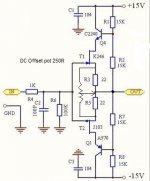
Or to use the buffer (attached), but this buffer is an unknown one and I wonder if it's output is able to drive the 800pf load it will see.
My next question is I have no idea how to sim circuits, can anyone sim this buffer I have (attached) which is availible on ebay for $10 to see if it can take up to 1000pf load on it's output without ringing or oscillating?
Cheers George
I have done some more study of the AD844 in open loop mode with it's own buffer as the output, and the data sheet says the buffer as it is, is good only for driving up to 100pf of capacitive load, up to 1000pf with the feed forward network they suggest, which if I read right limits the current output drivability if used.
I measured the capacitance of what I'm driving interconnects and inputs and I think it's around 800pf.
I have two options one to use the feed forward network AD suggests which I believe comprimises the current output of the 844.
Or to use the buffer (attached), but this buffer is an unknown one and I wonder if it's output is able to drive the 800pf load it will see.
My next question is I have no idea how to sim circuits, can anyone sim this buffer I have (attached) which is availible on ebay for $10 to see if it can take up to 1000pf load on it's output without ringing or oscillating?
Cheers George
Attachments
Last edited:
typically the C load limit is for closed loop operation - the C slows down the buffer, adds phase shift
can usally be stabilized with a series dcoupling R or ferrite bead - since the conrer frequency can be MHz there is little ausio consequence
can usally be stabilized with a series dcoupling R or ferrite bead - since the conrer frequency can be MHz there is little ausio consequence
typically the C load limit is for closed loop operation - the C slows down the buffer, adds phase shift
can usally be stabilized with a series dcoupling R or ferrite bead - since the conrer frequency can be MHz there is little ausio consequence
So are you saying jcx that in open loop operation which as you know is the way it's being used that the C load can be much higher than the 100pf stated without stability feedforward network?
Cheers George
Last edited:
Yes that's what jcx is saying. The capacitive load limit is not due to the current capability of the buffer so much as the phase shift that's introduced. In open loop operation you do not care about phase shift very much, if at all because it has no consequence.
Yes that's what jcx is saying. The capacitive load limit is not due to the current capability of the buffer so much as the phase shift that's introduced. In open loop operation you do not care about phase shift very much, if at all because it has no consequence.
So then because it's got short circuit protection, I can remove the series 47ohm I put in for safety sake, and let the output buffer drive direct from it's 15ohm source, even into a 800pf load without ringing or oscillation problems?
I know there's not much difference between 15ohm or 47ohm output impedance, but I always like the lower number if no problems arise.
Cheers George
There won't be oscillation from the loop feedback no, but there's always the possibility of parasitics (much higher frequency oscillations) where emitter followers are concerned so if I were you, I'd isolate with an inductor (or ferrite bead) with appropriate damping resistor. This will maintain the low output impedance at audio and give some protection against HF parasitics. To be even more conservative, add a snubber (series RC) at the buffer output as is done with power amps.
but there's always the possibility of parasitics (much higher frequency oscillations) where emitter followers are concerned so if I were you, I'd isolate with an inductor (or ferrite bead) with appropriate damping resistor. This will maintain the low output impedance at audio and give some protection against HF parasitics.
Like you explained way back post 15 http://www.diyaudio.com/forums/digital-source/227677-using-ad844-i-v-2.html#post3323415 but this time in series on the buffer output.
Cheers George
Yes, or here's a more explicit example in the schematic I've put up for an ESS output filter - http://www.diyaudio.com/forums/digital-line-level/227284-build-thread-diyinhk-es9018-dac-ebay-3.html#post3332420
In this example the opamp isn't open loop so more inductors are needed for stability. In your case probably just one or two is all that's required.
In this example the opamp isn't open loop so more inductors are needed for stability. In your case probably just one or two is all that's required.
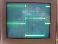
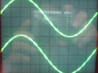
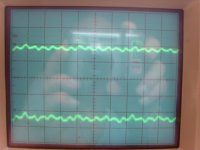
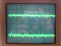
Here are some screen shots from my 200mhz Tek scope, sorry no flash too much reflection. PCM1704 to AD844, TZ to ground via 2.7kohm with 500pf across it 844's output buffer straight to output rca's which were loaded with 50kohms
The funny one for me is the spiral oscillation on the 20khz sine wave anyone seen anything like this?,this noise dissappers at 12khz sine waves. Then after I put away all the gear I though maybe it was my smp bench light that was doing it. Next time I'll see again.
1khz square wave 2v
20khz sine wave
Noise on output .1mV per division 20mhz scope filter bandwidth
Noise on output .1mv per division 200mhz scope bandwidth
Cheers George
Attachments
- Home
- Source & Line
- Digital Line Level
- Using the AD844 as an I/V