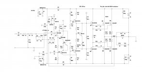
C9/C12 and parallel resistors 300K-2.2 Meg load of the voltage amplification stages of the power amplifier.Right on the ground. But it is also allowed on the power bus, which is less efficient.
Regarding post/schematic #994:
1) caps C9/C12 - I've seen some cases when this caps are connected to rails (not to GND), or (as in case for C12) to the collectors of drivers.
Maxim consistently uses GND. I used to use rails.
What is better/correct? Sim seems to work equally fine with both..
2) Speed-up cap between bases of output devices - not needed anymore? I guess not for Fets..
3) When testing/siming with square waves, adjustments of C5/R1 were usually needed - increasing either value was usually in order. Does it matter what do we increase? Capacitance vs Resistance?
1. Bruno has a AES paper about the evils of the classic Miller cap because it provides a path from the rail noise (and distortion) into the signal path. Same issue with C9/C12. But, I have seen fast transistor oscillate all by themselves when the Miller cap is not physically right on the transistor. I suppose if C9=C12 then the +rail noise cancels the -rail noise?
2. Normally I would always use a "speed up capacitor" but it seemed to slightly increase the THD so I dropped it.
3. Stabilizing an op-amp input requires that you choose either the op-amp dominant pole or the VAS, normally the VAS. To get the op-amp pole out of the way, you differentiate or ~short (low-Z) the op-amp output to prevent any voltage swing on the op-amp compensation. So the op-amp needs to drive a low Z or capacitive input. Related is something I omitted in my suggestions, is a pair of diode clamps between the op-amp output and negative input, limiting the op-amp output to +/-0.65V (except where you put feedback around the discrete stages that requires more op-amp voltage). This is related to clipping behavior.
Last edited:
>Related is something I omitted in my suggestions, is a pair of diode clamps between the op-amp output and negative input, limiting the op-amp output to +/-0.65V (except where you put feedback around the discrete stages that requires more op-amp voltage). This is related to clipping behavior.
D3 is there (at Q1) to control clipping.
D3 is there (at Q1) to control clipping.
After listening to the HexFet quasi amp for the whole day (I'm constantly switching amps..) I have to repeat my original assessment that it does sound better then LatFet version (1st amp built from this thread). Definitely stronger bass.
If anybody is interested in buildable Blomley, here is modified Hans Hartsuiker version,
slightly improved, that at least sims ok.
It has symmetrical rails - primary reason I gave up on 'regular' Blomley..
From what I remember Blomley was a good candidate to add servo to it to control output DC offset..
Hello, I can't open this ASC with Altium Designer or PADS 9.5. What is the problem? What software is used to open?
Maxim, so the latest schematic from posts #935 and #939 is kind of 'final', I guess?
Ready for PCB design?
==================
Максим, так что последняя схема из постов №935 и №939 вроде как «окончательная»? Готовы к проектированию печатной платы?
Ready for PCB design?
==================
Максим, так что последняя схема из постов №935 и №939 вроде как «окончательная»? Готовы к проектированию печатной платы?
Будь готов! Всегда готов.
Always ready.
The Board for 4 pairs of bipolar transistors is ready to order .
I'll just make some changes and that's it.
Эскиз . Sketch
Do you need overload protection ? How many pairs of exits ? 2 ? 4 ?
Always ready.
The Board for 4 pairs of bipolar transistors is ready to order .
I'll just make some changes and that's it.
Эскиз . Sketch
Do you need overload protection ? How many pairs of exits ? 2 ? 4 ?
Attachments
Last edited:
So these schematics are OK, no more changes expected?
I think I will design a board for complementary hexfets (2 or 3 pairs),
and perhaps I can make this board also to work out for quasi version.
Actually it doesn't matter - BJTs or Fets, PCB will be the same, just different values for compensation..
Quasi improvements with LEDs that Steve proposed look worth trying...
Question 1: what drivers you are going to use for your 4 pairs?
How many pairs drivers 2SC3503/2SA1381 can handle?
I think 4 would be too much, for more than 2 pairs I will need bigger drivers.
Question 2: Are you seriously planning to use higher rails for VAS stage?
I guess you care about efficiency..
====================
Значит, эти схемы в порядке, больше никаких изменений не ожидается? Думаю, я разработаю плату для дополнительных шестигранников (2 или 3 пары), и, возможно, я смогу заставить эту плату работать и для квази-версии. Собственно не беда - БЮТ или Фетс, ПП будут одинаковыми, только разные значения компенсации .. Квази-улучшения со светодиодами, которые предложил Стив, выглядят достойно того, чтобы попробовать ...
Вопрос 1: какие драйверы вы собираетесь использовать для своих 4 пар? Со сколькими парами могут справиться драйверы 2SC3503 / 2SA1381? Я думаю, что 4 будет слишком много, для более чем 2 пар мне понадобятся драйверы большего размера.
Вопрос 2: Вы серьезно планируете использовать более высокие рельсы для этапа VAS? Думаю, вы заботитесь об эффективности ..
Power supply 40volt VC .UN -50volt. For 3 pairs of a1943/C5200 Bipolars, the a1837/C4793 pair was enough . The First Is A1380/C3502.Everything worked perfectly in the monster.
What are the dimensions of your PCB?
Great spirit ! 🙂
Great spirit ! 🙂
Attachments

Last edited:
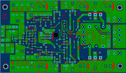
I checked the max size of my aluminum chassis - looks like I will build 2 pairs of outputs (per channel) version. But I need all power transistors to be lined up on one edge of the PCB.
I don't want this whole amp to be bigger/wider than my last 2 builds (Wiederhold Quasi), which comes to 32cm (width) by16cm (depth).
2SC3503 / 2SA1381 will be fine for 2 pairs.
So I guess I'll design my own PCB...
================
Я проверил максимальный размер своего алюминиевого корпуса - похоже, я сделаю версию с двумя парами выходов (на канал). Но мне нужно, чтобы все силовые транзисторы были выровнены на одном краю печатной платы. Я не хочу, чтобы весь этот усилитель был больше / шире, чем мои последние 2 сборки (Wiederhold Quasi), которые составляют 32 см (ширина) на 16 см (глубина). 2SC3503 / 2SA1381 подойдет для 2 пар. Думаю, я спроектирую свою собственную печатную плату ...
How long ago it was.in 1966.
Yeah, time goes too fast.. So many changes since then.
I checked the max size of my aluminum chassis - looks like I will build 2 pairs of outputs (per channel) version. But I need all power transistors to be lined up on one edge of the PCB.
I don't want this whole amp to be bigger/wider than my last 2 builds (Wiederhold Quasi), which comes to 32cm (width) by16cm (depth).
2SC3503 / 2SA1381 will be fine for 2 pairs.
So I guess I'll design my own PCB...
================
Я проверил максимальный размер своего алюминиевого корпуса - похоже, я сделаю версию с двумя парами выходов (на канал). Но мне нужно, чтобы все силовые транзисторы были выровнены на одном краю печатной платы. Я не хочу, чтобы весь этот усилитель был больше / шире, чем мои последние 2 сборки (Wiederhold Quasi), которые составляют 32 см (ширина) на 16 см (глубина). 2SC3503 / 2SA1381 подойдет для 2 пар. Думаю, я спроектирую свою собственную печатную плату ...
This is possible, though less optimal. I think everything will work out
Yeah, time goes too fast.. So many changes since then.
Давно.
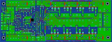
So this is the schematic I'm going to design PCB for.
If I have enough space, will also try to accommodate quasi version on the same PCB.
This should be good for BJTs and HexFets.
Basic differences between Maxim's and mine will be:
a) same rails for all stages (no higher rails for VAS)
b) double output transistors vs triples
c) support for BJT/HexFet complementary/quasi on the same PCB
d) less filtering capacitors (I want to make it small..)
e) output RL no implemented (I have it on the speaker protection board)
Values of some elements may still change...
Attachments
Last edited:
- Home
- Amplifiers
- Solid State
- Unusual amp from 1987