For sure the comparator solution works, just wanted to say, that a bit more hysteresis might be useful. (For not false triggering)
Guys, thanks for all the feedback.
I have updated the schematic to include the feedback as well as a couple more optimisations:
- TPA ICs setup in master / slave mode (to ensure minimum oscillator interference)
- Passive out of band filters on the inputs including DC decoupling
- Single earth and a simpler power supply. Rob was correct - trying to keep a split supply made it too complex and potentially would detract from the sonics. I adopted the charge pump idea for the negative rail and with regulation & low current draw is a better solution.
- Added more diodes for 1.5v hysteresis for the voltage supervisor
- Decreased the opamp resistor values to reduce noise
- Cleaned up the schematic so it is easier to read.
I think this is about it - do have a final look to see if I have forgotten anything!
Dean
Attachments
Guys, thanks for all the feedback.
I have updated the schematic to include the feedback as well as a couple more optimisations:
- TPA ICs setup in master / slave mode (to ensure minimum oscillator interference)
- Passive out of band filters on the inputs including DC decoupling
- Single earth and a simpler power supply. Rob was correct - trying to keep a split supply made it too complex and potentially would detract from the sonics. I adopted the charge pump idea for the negative rail and with regulation & low current draw is a better solution.
- Added more diodes for 1.5v hysteresis for the voltage supervisor
- Decreased the opamp resistor values to reduce noise
- Cleaned up the schematic so it is easier to read.
I think this is about it - do have a final look to see if I have forgotten anything!
Dean
Hi,
Looks better.
Two remarks. You have 3R3 resistors in the +12V line of the GVDD, but the reference design put the 3R3 in the VDD line only. Any reason to change this?
The LM317 is now dissipating a lot of power... 24VAC gives about 32V, so the regulator takes 20V, the +12V needs about 100mA per chip, so 200mA in total. This is 4W, needs big heat sink. I see TO92 in the diagram, 4W is not going to happen with a TO92... TO220 with a big heat sink will work.
But to save power, maybe consider the switching regulator from the reference design?
Rob
Thanks Rob.
I have been working off the datasheets and it does look like the datasheet and reference design conflict (d/s has 3R3 in the +12v GVDD line). I see a post on TI E2E commenting on the discrepancy. I'll change to the reference design.
Also good pickup on the LM317 - I didn't check the current draw for the +12v, not expecting it to be that much as it doesn't power the main drive. Ivdd and Igvdd is 90mA according to the datasheet however when adding the current used by the opamps it will be around 250mA total, so the regulator has to swallow 5W, too much.
I also tried modelling splitting the power supply and having the output of the bridge rectifiers in series with +15v being accessible from the bottom supply however both the charge pump and the Vgg supply would add significant load to the bottom supply as well as doubling the ripple/noise from both supplies to the +30v rail. So I'll implement a switcher.
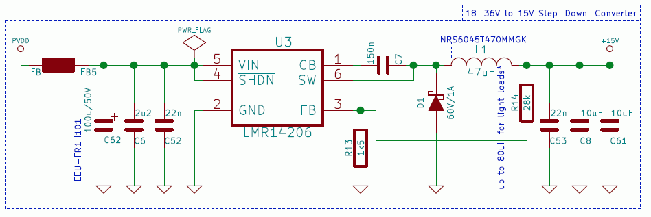
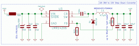
I used an LMR14206 here to get down to 15V following LM317 with additional (optional) capacitance multiplier.
Hi Dug, nice compact part - although my local parts house (rs-components) doesn't stock it.
doctormord - yep, this looks like the best solution (simple switcher with linear reg to quieten the 12v rail.
doctormord - yep, this looks like the best solution (simple switcher with linear reg to quieten the 12v rail.
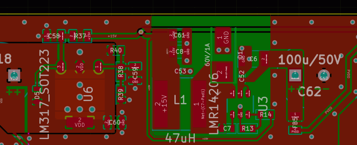
If using this IC, layout is somwhat critical.
Part of my schematic:
Layout:
Part of my schematic:
Layout:
Attachments

Last edited:

Here is a try at a PBTL. I will have the boards next week.
Looking good!
Regards,
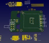
Here is the final schematic for my 'quality' 2.1 system which includes fault indicators. A bit more complex than I first envisioned using a single TPA for 2.1 output but it should sound better. After all components are cheap & so is Elecrow PCB's 100x100mm service....
I'll post the PCB layout a little later - careful layout for grounding / planes will be important for optimal performance.
I'll post the PCB layout a little later - careful layout for grounding / planes will be important for optimal performance.
Attachments
Here is a try at a PBTL. I will have the boards next week.
Will this be a 2oz board?
Will this be a 2oz board?
LOL (I actually did), no.
I am almost ready to power up my first board.
Built some loads...dual 4R.
Last edited:
Here is the final schematic for my 'quality' 2.1 system which includes fault indicators. A bit more complex than I first envisioned using a single TPA for 2.1 output but it should sound better. After all components are cheap & so is Elecrow PCB's 100x100mm service....
I'll post the PCB layout a little later - careful layout for grounding / planes will be important for optimal performance.
Some notes/questions:
- Wouldn't it be better to decouple the pots from DC with 2 additional caps?
- Are you sure to come along with an 1.5A regulator, quiescentcurrent is already ~150-200mA
- You may want to have impedance matching resistors in your clock lines
- By that you can also implement slave mode switching1/2 (+/+ -/- or +/- -/+ (Datasheed 10.2.1.2.4)
- Why are you using JFets+Pullups+Zenners? (Why not 😀 )
- You may want to increase CStart later (up to 680nF), have your footprint ready for that
- Schematic readability would greatly improve if more GND-symbols are used rather than having extra long GND-wires
- FREQ_ADJ of slave must be connected to DVDD not GVDD
- You want to have the series diodes behind the cap of your LC-Filters to work properly
Keep it up.
Regards, Christian
Last edited:
If the 1.5A regulator is being used to regulate the PSU for only the left and right channels (that will presumably be high passed anyway) then I don't really see the problem. These are going to be used near field and wont realistically need much power. Very quick transients will be provided for by the local decoupling.
I've powered my TPA3118 board on my near field set up a number of times from the bench PSU and when watching the current draw on music signals...I never get anywhere close to 1.5A even with it turned up loud.
1.5Amps is more than enough for 2x boards +12V supply though. I used 2x LT3042s in parallel for the +12V supply on three chips.
Thanks everyone for the feedback, its appreciated and will help me learn and have a better end result.
Added 33 ohm resistors in the clock lines for impedance matching.
Regarding slave mode 1 / 2 switching, I'm unclear what the benefits are of switching polarity, I assume if there are multiple slaves attached (I only have 1 slave). I have implemented slave model 1 +/+ -/-
Regarding the comment about the series diodes behind the cap for the LC filter not working, it is actually a CLC filter and the diodes are between the L and the second C so it should work. Idea here is to stop the high power subwoofer amp from draining the power from the regulator caps during transients. I'm open to suggestions of doing this a better way.
Regarding 1.5A regulator, 5th Element sums it up, the near field speakers will be crossed over at 100Hz and never ask more than 5w from the amp, most of the power supplied by the 2200uF local decoupling. But I'll swap out for the 3A regulator just in case.
The schematic is a little messy and I'm no artist - I use kicad which does a decent job with the schematic layout but takes some effort to move labels about and I tend keep the layout too bunched up. However the schematic isn't the end result - I'd rather spend the time on getting the PCB layout perfect. Point taken about using more GND symbols.
Regarding caps on the pots, I'm not sure they are needed as I already AC couple the inputs and any quiescent bias DC from the opamps should be minimal? I'd prefer to keep caps out of the signal path as much as possible (the main reason I'm using two TPA chips so that I avoid an electro in the output when using SE configuration). These pots will be set and forget not a regularly used volume control as volume will be set in the source (a PC). So 'scratchiness' caused by DC on the pot long term shouldn't be a problem and the current amp I have been using for years that this design will replace uses a similar scheme and the pots are dead silent. However I'm happy to hear of other reasons to AC couple the pots.
FREQ_ADJ for the slave needs to be +3.3v (DVDD) not +12v so this is an error in my schematic - fixed.
Regarding JFET and zeners, I'm copying the user guide schematic which has a separate 3.3v power supply. Note the error outputs are hi-z so need a 3.3v pullup and I didn't want to load DVDD. I don't understand why the user guide uses a FET to switch the error LED current to ground for the off-state, seems like a waste of power.
LM46002 for improved EMI performance - hadn't thought about that. LM4562's are high performance opamps and I have a stash of them from 10 years back when they first came out. If LM46002 will outperform them due to the large amount of EMI from all the power switching I'll swap over (or be more careful with layout of the LM4562).
Attachments

When operating two chips in master/slave, the point of having the out of phase option is so that when both chips are switching, one chip switches positive as the other switches negative, helping to even out demands placed upon the power supply.
This is only concerning the hard switching of the class D output stage (as one chip switches on the other switches off) and has no effect on the phase of the analogue output.
This is only concerning the hard switching of the class D output stage (as one chip switches on the other switches off) and has no effect on the phase of the analogue output.
- Home
- Amplifiers
- Class D
- TPA3251d2