----------------------------------------------Hi again ... I have taken the liberty of cutting & pasting from Andrea's schematics. It basically looks like this ...
Cheers,
Jesper
Ok, good:
For the lowest "jitter" you need to go for the fastest logic, preferably 74AC series.
However, these are difficult to work with.
If u dont have the proper tools or not familiar with rf design, just use 74HC74 (these are actually quite good).
Replace the 74hc04 inverter after the oscillator with a decent buffer.
I'll try to find something.
Add a resistor ~ 100 ohms right after the osc output before the latch input.
Replace the inverter-based Pierce with a discrete one, again, i'll try to find something...
....In the mean time everyone is welcome to help support Jesper and Andrea with design ideas for an exellent discrete Pierce oscillator.
Last edited:
Buffer Amp for 5.6 MHz
Allright...
I found this one on Wenzel's home page.
Quite interesting, values adjusted for gentlevoice's 5.6 MHz oscillator.
Simple, effective, designed to do the job - no inverters.
Cheers...

Allright...
I found this one on Wenzel's home page.
Quite interesting, values adjusted for gentlevoice's 5.6 MHz oscillator.
Simple, effective, designed to do the job - no inverters.
Cheers...
Last edited:
Hi Alexiss: Thanks for the suggestion. However, as I wrote 😉 I have only 6.7 - 6.8 VDC available and also it's a 6.144 MHz crystal - not a 5.6 MHz crystal ... I think you've been reading quickly 😛
That said - can I ask you why you find this buffer interesting? To me it looks somewhat complex and also with many components in/around the oscillator path ...
However, I'm curious here and found this Pierce-style-oscillator example on the internet (attached). I've drawn up the circuitry in LTSpice (a .asc file) so maybe I can ask you to "fill in the blanks" in terms of values and add possible improvements? Please remember the 6.8 VDC limitation.
I know this is with a short notice but I have to continue with my design early tomorrow (already late) so I can only wait a little ... And, as it is I have confidence in Andrea's approach/circuitry so if a discrete oscillator cannot be done by now I'll continue with his design and await a possible later chance at a discrete Pierce oscillator.
Have a good evening,
Jesper
Attachments
In the words of Jocko;
You want to use logic that is as fast as you need, and no faster.
I just rebuilt my CD player using one of his clocks and I'm thrilled.
He's been preaching much of what is finally being posted here, for years. Low noise, below 10Hz, is the all important number.
You want to use logic that is as fast as you need, and no faster.
I just rebuilt my CD player using one of his clocks and I'm thrilled.
He's been preaching much of what is finally being posted here, for years. Low noise, below 10Hz, is the all important number.
In the words of Jocko;
You want to use logic that is as fast as you need, and no faster.
You are correct, but this is not a very precise statement.
In reference to JITTER, the signal converter should be as fast as possible.
So more precisely stated, how fast should the clock flanks be?
The other peripheral factors dictate what will be needed in that particular circuit.
I think I mentioned something about this earlier on the thread here.
...He's been preaching much of what is finally being posted here, for years. Low noise, below 10Hz, is the all important number.
I know, he is great.
Best wishes
Hi Alexiss: Thanks for the suggestion. However, as I wrote 😉 I have only 6.7 - 6.8 VDC available and also it's a 6.144 MHz crystal - not a 5.6 MHz crystal ... I think you've been reading quickly 😛
That said - can I ask you why you find this buffer interesting? To me it looks somewhat complex and also with many components in/around the oscillator path ...
Jesper
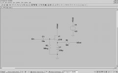
We aim to please...
2 resistors, 1 inductor, 1 cap, 6.1 MHz, Vdd = 6.8 Vdc. (R1 may be eliminated to: 1 resistor, 1 inductor, 1 cap).
If you really want to go at it, you can eliminate c1, R1, R3 and the circuit would still function but
the output DC voltage of the previous stage should be known
and you may need to add an appropriately sized resistor in the Source-path of the active jFET.
The circuit would then become: 1 jFET + 1 inductor
Attachments
Last edited:
...I found this Pierce-style-oscillator example on the internet (attached).
Can I ask you to "fill in the blanks" in terms of values and add possible improvements? Please remember the 6.8 VDC limitation.
Jesper
This version will not be that different from an inverter-based Pierce. The Pierce designed by Andrea is actually very good.
I keep forgetting that many fellow diy:ers want SIMPLE circuits with excellent performance. Sorry.
Last edited:
Thanks Alexiss for the feedback & "simplifying" the buffer ... It looks interesting to me - will consider it 😉 .... I may have missed something though which is what you will put in front of the buffer?
Would it look like the attachment (orange area the pierce like Andrea has outlined)?
Cheers & thanks again,
Jesper
Would it look like the attachment (orange area the pierce like Andrea has outlined)?
Cheers & thanks again,
Jesper
Attachments
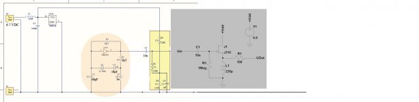
.... I may have missed something though which is what you will put in front of the buffer?
Jesper
Something like this:
Attachments

Tackar så mycket, Alexiss for the schematic and comments 🙂 Now time to ponder and get a feel for what to do ...
Cheers to you,
Jesper
Cheers to you,
Jesper
@Alexiss: I think what I'll do is to make one each of the Driscoll, Pierce (Andrea's version) and then your version with the discrete buffer. And then I'll compare them. Layout-wise I've made the Driscoll and Andrea's Pierce version already so it should be accessible to do a discrete buffer version as well. In practice it will take a little while though as I have a vacation coming up.
However, I've also come to think of a potential "challenge" to this setup this morning. As it is the oscillator (i.e. the FF after the oscillator ) will feed into 6 converter gates. With e.g. a 5 ns effective rise time and a 60 ohm resistor on each converter "leg" the peak load on the FF output (or a buffer) will be just about 38 mAs (taking into account trace inductances and capacitances). Which may not be a challenge in theory (looks as if the peak currents are acceptable to CMOS ICs) but have you any experience with how this may affect jitter/phase noise figures in practice? And in case I consider placing a J310 buffer after the FF its IDSS of 24 mA (typ.) will be too low unless it is significantly increased ...
Another option may be to reverse the sequence of the FF and the buffer/inverter so that the oscillator itself feeds into the FF and then - subsequently - into an inverter/suitable buffer ... This would remove the load from the FF to an inverter/buffer (here assuming that FFs and inverters have similar characteristics) which I reckon could be beneficial ... ?
Any chance you have experiences/suggestions with this that you can share?
Hmmm ... this is a "general" comment to you and all helping out here - I know I'm asking many questions but as this is not the field where I know most I really do appreciate your help ...
Cheers 😉
Jesper
A P.S. to Alexiss: With the converter type I'm using I need to be able to control the duty cycle of the oscillator so that no oscillator noise affects the converter. To this end Andrea's duty-cycle network - or something similar is required. I reckon this may work with the buffer you outlined yesterday as well - although maybe not "optimal" from a simplicity point of view?
Last edited:
@Andrea:
With a reference to my previous post just above I hope I can I ask you this: In my case - where I use a FF to divide the clock - wouldn't it in the Driscoll oscillator case make sense to eliminate the inverter and place the FF where the inverter is now (I will not be using the 47k load resistor)? It would make for a shorter and potentially less jittery signal path ...
Cheers,
Jesper
@Alexiss: I think what I'll do is to make one each of the Driscoll, Pierce (Andrea's version) and then your version with the discrete buffer. And then I'll compare them.
Well, I am a little uncertain of your design goals.
I have to remind you that the simplified buffer (the last schematics) has some compromises built into it.
This is because you needed simplicity. The best one would be the first buffer.
...the FF after the oscillator [/B]) will feed into 6 converter gates. With e.g. a 5 ns effective rise time and a 60 ohm resistor on each converter "leg"
...but have you any experience with how this may affect jitter/phase noise figures in practice?
That depends (among other things) on the Input Referred Noise Density of whatever stage(s) you're using the FF to feed.
But generally you will increase the potential for higher jitter generation with such a load.
..Another option may be to reverse the sequence of the FF and the buffer/inverter so that the oscillator itself feeds into the FF and then - subsequently - into an inverter/suitable buffer ... This would remove the load from the FF to an inverter/buffer (here assuming that FFs and inverters have similar characteristics) which I reckon could be beneficial ... ?
If u think that then I have failed to get my message across. It's probably my bad explanations.
Hmmm ... this is a "general" comment to you and all helping out here - I know I'm asking many questions but as this is not the field where I know most I really do appreciate your help ...
I am really uncertain about your design goals, and I apologize for that.
Your setup (as I've understood it - I maybe wrong) is really sub optimal with regards to jitter.
You have everything you need on this thread to build a really low jitter/phase noise/timing inaccuracy system.
My advice would be to keep things simple, and use Andreas designs.
A P.S. to Alexiss: With the converter type I'm using I need to be able to control the duty cycle of the oscillator so that no oscillator noise affects the converter. To this end Andrea's duty-cycle network - or something similar is required. I reckon this may work with the buffer you outlined yesterday as well - although maybe not "optimal" from a simplicity point of view?
I do not understand this, I'm sorry. What is the duty cycle setup?
I'm not sure you would want to control the Duty Cycle of the clock pulses.
Last edited:
...That depends (among other things) on the Input Referred Noise Density of whatever stage(s) you're using the FF to feed...
A typo mistake in the text above.
What I meant to say was:
Input stage Equivalent Noise Bandwidth of whatever stage(s) you're using the FF to feed...
Srry, I'm s tired these days... :-(
Last edited:
Hi Alexiss ... I'll send you a PM tomorrow morning ...
Cheers,
Jesper
Hmmm... wishing you some (for you good) energy for the day ;-)Srry, I'm s tired these days... :-(
Cheers,
Jesper
Hmmm... wishing you some (for you good) energy for the day ;-)
Cheers,
Jesper
----------------------------------------------------------------------
Thanx, there is lots to do at work :-(
Anyways, looking at the Inverter-based Pierce designed by Andrea, it is actually very good indeed.
Specially equipped with the Laptech xtal, I think it is an interesting design for the fellow diy:ers, specially due to its simplicity, guaranteed functionality, and high performance.
But I think the RutgerS oscillator would perform way better with the same Laptech xtal.
I am not sure, but I think Andrea is now using the 74hcU04 inverters that are single stage designs, leading to massive sonic improvement over the original.
It was a very interesting listening test that Andrea performed.
Unfortunately he did not perform any listening with the RutgerS oscillator (which I think would score very high with 74hcU04).
Any chance of doing that Andrea?
Attachments
Last edited:
The crystals have been ordered to Laptech (and paid in advance) but they have not yet told me the date of delivery.
I expect to receive the crystals within the end of April. Then I will ship them to all the members.
Andrea,
Did I miss something? It is already september and I still did not receive any Xtal....
Herbert.
Andrea,
Did I miss something? It is already september and I still did not receive any Xtal....
Herbert.
Hi Herbert,
I don't remember any order from you. I received your request for a 12.288 MHz AT-Cut crystal in June by email, but I cannot reply to your email address because your mail server refuses my messagges as spam. I sent you a PM, please check your incoming PM.
Andrea
----------------------------------------------------------------------
Thanx, there is lots to do at work :-(
Anyways, looking at the Inverter-based Pierce designed by Andrea, it is actually very good indeed.
Specially equipped with the Laptech xtal, I think it is an interesting design for the fellow diy:ers, specially due to its simplicity, guaranteed functionality, and high performance.
But I think the RutgerS oscillator would perform way better with the same Laptech xtal.
I am not sure, but I think Andrea is now using the 74hcU04 inverters that are single stage designs, leading to massive sonic improvement over the original.
It was a very interesting listening test that Andrea performed.
Unfortunately he did not perform any listening with the RutgerS oscillator (which I think would score very high with 74hcU04).
Any chance of doing that Andrea?
The Colpitts-Clapp oscillator still uses the old buffer with gates in series/parallel, I have not yet updated the PCB layout.
I have not listened to this oscillators because I have not yet found the time to build it at 22 Mhz. I will do the test in the next weeks, as soon as I will find the time.
The Colpitts-Clapp oscillator still uses the old buffer with gates in series/parallel, I have not yet updated the PCB layout.
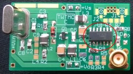
I just saw the picture of the recent TWTMC-C pcb and it features a Potato 74GU04? but maybe it's a triple cascaded inverter.
I have not listened to this oscillators because I have not yet found the time to build it at 22 Mhz. I will do the test in the next weeks, as soon as I will find the time.
I'll be looking forward to this test. I think yu will find this setup (RutgerS + Laptech + 74HCU04) as sonically the best alternative so far, maybe even better than the Driscoll.
Good luck.
Attachments
Last edited:
- Status
- Not open for further replies.
- Home
- Source & Line
- Digital Line Level
- The Well Tempered Master Clock - Building a low phase noise/jitter crystal oscillator