............t6(bc182) could be a problem............base- emitter shorted...........
greets
Just emitter and colector of T6(BC182B) are reverted on schematics in post #1. Base-colector should be shorted and emitter connect to 6V zener. T6(BC182B) is used as diode for thermal compensation reff voltage of CCS. T6(BC182B) and T9(MPSA93) can be replaced with 1N4148 diodes.
Last edited:
jam:
from my experiments with the amp designs in the early 80's Hitachi Power MOSFET databooks (very much like HMA-7500, etc), i've seen this too.
folks need to remember this topology was recommended for use with lateral mosfets because the designers' wanted LOTs of open loop to reduce the lateral MOSFETs distortion which they attributed to low transconductance.
mlloyd1
Nagsy,
...
I am trying to point out that this design rings badly into a reactive load, I observerd it to ring into a purely resistive load all pointing to the fact that the amp is on the verge of instability.
Jam
Alex's new schematic is correct now. Please do not make it confusing. My original schematic on page one is also correct regarding this issue.
The Base and Emitter should be shorted on the Motorola BC182B and the 6V Zener diode's cathode end should be connected to the Collector.
I have three separate Goldmund A1 block modules right smack in front of me. So unless they made a mistake in 3 different amplifiers (which I know they didn't) this is correct.
Alex's latest schematic is also correct.
Last edited:
Just emitter and colector of T6(BC182B) are reverted on schematics in post #1. Base-colector should be shorted and emitter connect to 6V zener. T6(BC182B) is used as diode for thermal compensation reff voltage of CCS. T6(BC182B) and T9(MPSA93) can be replaced with 1N4148 diodes.
This is basic electronic, good luck you need it😉
Alex's new schematic is correct now. Please do not make it confusing. My original schematic on page one is also correct regarding this issue.
The Base and Emitter should be shorted on the Motorola BC182B and the 6V Zener diode's cathode end should be connected to the Collector.
I have three separate Goldmund A1 block modules right smack in front of me. So unless they made a mistake in 3 different amplifiers (which I know they didn't) this is correct.
Alex's latest schematic is also correct.
You have three separate Goldmund A1 block modules, but you don't have amplifier, this modules must have mistake and was replaced. I just want to help not confusing you.
Last edited:
apexaudio - I understand your point. However, this is not what Goldmund does in their amplifiers.
Again, I have 3 Goldmund A1 modules right in front of me as I type this. The cathode end of the 6V Zener diode is connected to leg 1 on the Motorola BC182B. Here's the datasheet for Motorola's BC182B: BC182B pdf, BC182B description, BC182B datasheets, BC182B view ::: ALLDATASHEET :::
As you can see, leg 1 on the BC182B is the Collector. Legs 2 (Base) and 3 (Emitter) are shorted in the Goldmund A1 module. Would you like me to take a detailed picture for you?
NagysAudio
There are numerous OTHER amplifiers on this forum that have the base tied to the collector to form a diode in the input stages of those amps.
Just look at a few other examples and I think you will see that what Apex is saying is totally valid. Apex is trying to help all here.
The fix is easy for those that want to try it another way, just flip the transistor 180 degrees and all is well. Those that don't want to can install as is. Simple
Last edited:
I have two Goldmund amplifiers, Mimesis 6 (2 modules) and Mimesis 3 (4 modules). I also obtained an additional 2 from a repair shop and 1 from Goldmund directly. I have a total of 9 working A1 modules. I unpotted 3 of them. What are the chances that I just happened to unpot 3 modules out of 9 that had a mistake?
I understand that he is trying to help and I completely understand the theory to connect the Base and Collector. But that is just not what Goldmund does. And this is a Goldmund schematic.
CCS can work without thermal compensation, just with 6V zener without T6(BC182B). And that was hapen with reverted polarity of T6(BC182B).
apexaudio - The schematic can work both ways theoretically. The Base and the Collector can be shorted on the T6 Motorola BC182B and the 6V Zener diode's Cathode connected to T6's Emitter (WRONG WAY). Or the Base and Emitter can be shorted on the Motorola BC182B and the 6V Zener diode's Cathode connected to T6's Collector (RIGHT WAY).
Just as an example, if connected like in the original Goldmund Schematic (posted on page one): Lets say we have -60V on the Anode end of the 6V Zener diode, then we should have -54V on the Collector of T6, -55V on the Emitter of T6, and -56V on the Emitter of T5.
Now if it's connected the WRONG WAY, like some of you insist it should be, with Base and Collector shorted on T6 and 6V Zener diode's Cathode connected to T6's Emitter: Lets say we have the same -60V on the Anode end of the 6V Zener diode, then we should have -54V on the Emitter of T6, -53V on the Collector of T6, and -54V on the Emitter of T5.
You will have slightly different voltages and throw the circuit off balance. The amp might EVEN work both ways, but it will work more correct in how Goldmund has T6 and the 6V Zener diode connected.
apexaudio, you're assuming that if the Base and Emitter are shorted on T6 that it will act as if it's no longer there in the schematic and that's a false assumption.
Further, the protection diodes D2 (ZD12V), D5, D4, and D3 (ZD12V) are once again connected the wrong way in Alex's schematic. They are connected the RIGHT way in the schematic that I posted on page one and in the original Goldmund schematic. The way they're connected right now is nonsensical. I don't feel like explaining the entire theory why they're connected the way they are, because it will take too long. But trust me, Goldmund is correct! The way these diodes are connected right now, it's as if they're stabilizing the AC signal to BSS71/BSS74 to 12V. What kind of sense does that make?
Alex, can you please, please connect them like they are in the original schematic. That is the correct way.
There are a few certain individuals that keep on posting false information and are trying to mislead the potential builders of this amplifier. Please stop. Please stop posting schematics for other amplifiers, because this is a schematic for a Goldmund amplifier. Not Hafler, etc. I don't care how they connect parts in their schematics. Every schematic is different.
Regarding the MOSFETS. Some of you said that having +/-80V power supply was too high for 160V rated MOSFETS. Again, this is a misinformed opinion. This is a 250W amplifier. With an 8ohm load, you can expect +/-45V, or so. 80V+45V=125V max on the MOSFETS. Please learn the Ohm's Law and how to add properly.
Last edited:
I have two Goldmund amplifiers, Mimesis 6 (2 modules) and Mimesis 3 (4 modules). I also obtained an additional 2 from a repair shop and 1 from Goldmund directly. I have a total of 9 working A1 modules. I unpotted 3 of them. What are the chances that I just happened to unpot 3 modules out of 9 that had a mistake?
Apex, we know that there are many kinds of ccs, and they have MICRO difference. The question to you is, what difference does it make to connect it the way Goldmund does? I know the transistor doesn't function as a transistor there, but McGyver may know something?
With such a strange arrangement, will it give a certain amount of temperature coefficient? If so, remember that they (the front end) are potted with special compound, and I heard about dedicated heatsinking (?). Could it be just an attention to detail of the implementation?
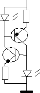
Because we might have different implementation, how about this kind of ccs (attached)?
Attachments
Jay - apexaudio is just plain wrong here and that's that. Yes, the input stage is potted, but that means nothing. All new goldmund amplifiers still use the same module only that it's completely unpotted. So the amp will work properly both ways, weather it's potted, or not. There are no heatsinks of any kind in the input stage.
Just as an example, if connected like in the original Goldmund Schematic (posted on page one): Lets say we have -60V on the Anode end of the 6V Zener diode, then we should have -54V on the Collector of T6, -55V on the Emitter of T6, and -56V on the Emitter of T5.
You were faster to give the answer there. But I still don't understand, how can it be -55V on the emitter of T6? I know that Vbe can be 0v7-1v but Vbc or Vce?
Regarding the MOSFETS. Some of you said that having +/-80V power supply was too high for 160V rated MOSFETS. Again, this is a misinformed opinion. This is a 250W amplifier. With an 8ohm load, you can expect +/-45V, or so. 80V+45V=125V max on the MOSFETS. Please learn the Ohm's Law and how to add properly.
May be it is just about... I don't know. May be there's possibility that when many bad things happen at the same time the mosfet will fail below its stated "SOA"? I believe that there is that risk. Can you find a clipping indicator in the original Goldmund? (that can be used to control overuse of the power of the amplifier)
Again, T6 can be connected either way. But if you connect it the way apexaudio suggests, then you'll have slightly different voltages and it might unbalance the circuit. If that's what you want, please go ahead and do it. I will build it the proper working way, as been proven in the 2 Goldmund amplifiers that I listen to almost everyday.
You will have 6V on 3k emitter resistor of T5, and CCS give 2mA either way. Without thermal compensation 6V +/-0,002V per degree, so change of 50deg give 0,1V change Vbe on T5, less than 1% current change of CCS.
Last edited:
I could open my amps up and measure all the voltages, but I just don't feel like it. I know how it's supposed to be connected and I feel like it would be a waste of my time. Same goes for any theoretical calculations.
Here's a picture I posted a few days ago, you can even see in it where the Zeners are connected. Please look on the left top side of the module. Remember, Motorola BD182B is as follows: Leg 1 = Collector, Leg 2 = Base, and Leg 3 = Emitter. You can tell in the picture, in both modules, the Base and Emitter legs are joined and soldered to a single pin. The Zener is soldered to the same pin as the Collector leg.
Here's another picture I found online. This is from a recent Goldmund (no more than a few years old) with unpotted modules. This pic is for orientation purposes. See the 6V Zener diode, its black stripe (Cathode) is pointing to the Motorola BC182B transistor.
And this is of the module's bottom. Please look at the top right corner. The 6V Zener diode's legs are straddling the surface mount resistor. The track goes through the 3K surface mount resistor and to Leg 1 of the BC182B transistor, which is the Collector. Leg 2 (Base) and Leg 3 (Emitter) are clearly connected together by the circuit board tracks.
I have examples of 3 modules from the 80s/90s and one module from the 00s. All are connected the same CORRECT way. I wasted enough time on this. If anyone takes bad advice and builds this amplifier incorrectly, you can ask jam and apexaudio for help in sorting things out.
Here's a picture I posted a few days ago, you can even see in it where the Zeners are connected. Please look on the left top side of the module. Remember, Motorola BD182B is as follows: Leg 1 = Collector, Leg 2 = Base, and Leg 3 = Emitter. You can tell in the picture, in both modules, the Base and Emitter legs are joined and soldered to a single pin. The Zener is soldered to the same pin as the Collector leg.
An externally hosted image should be here but it was not working when we last tested it.
Here's another picture I found online. This is from a recent Goldmund (no more than a few years old) with unpotted modules. This pic is for orientation purposes. See the 6V Zener diode, its black stripe (Cathode) is pointing to the Motorola BC182B transistor.
An externally hosted image should be here but it was not working when we last tested it.
And this is of the module's bottom. Please look at the top right corner. The 6V Zener diode's legs are straddling the surface mount resistor. The track goes through the 3K surface mount resistor and to Leg 1 of the BC182B transistor, which is the Collector. Leg 2 (Base) and Leg 3 (Emitter) are clearly connected together by the circuit board tracks.
An externally hosted image should be here but it was not working when we last tested it.
I have examples of 3 modules from the 80s/90s and one module from the 00s. All are connected the same CORRECT way. I wasted enough time on this. If anyone takes bad advice and builds this amplifier incorrectly, you can ask jam and apexaudio for help in sorting things out.
Last edited:
- Home
- Amplifiers
- Solid State
- The Very Best Amplifier I Have Ever Heard!!!!