Stochino's amp is class A/B with a slew rate of over 300V/us and a very high bandwidth. It uses VFET outputs, sounds very, very good and is stable.
Look like everyone has come to the conclusion that this amp is "on the edge".
75 degrees margin is acceptable as Keen posted with a LCR network in place. I saw very strong ringing with high power square wave test at 10uF/10khz. Bumping Cdoms up from 4.7pf to 22pF solved this without compromising too much bandwidth (900k). Phase margin was 85 degrees at this point , a "sweet spot" I normally shoot for which will even remain stable without a output network.
So this comes down simply to whether you want to trade bandwidth for long term reliability. This decision would really require actual prototyping , scope and subjective assessment. I personally would do this after reading of the goldmund
on the web.
On the subject of the OP inductor being essential for stability , I feel it should be looked at as "insurance".
OS
Last edited:
Good thing Borbely is closing shop. (DC-100=>DC-102)
(maybe the shadow turned singing detective ? )
)
(maybe the shadow turned singing detective ?
)I hope he flogs off his stash, but freebie hand-outs for prosperity is fine too.
Hang on, he could write a book (like the singing detective, while peeling skin off in the dungeon)
Hang on, he could write a book (like the singing detective, while peeling skin off in the dungeon)
I actually sent him an email begging him to write a book.
The guy has to be one of the most humblest men around considering how much he knows.
The guy has to be one of the most humblest men around considering how much he knows.
Anyway I might be still interested to build this amp. I am sure it is a good amp, but it will be definitely interesting to see how it compares to my other amps.
Anyway I might be still interested to build this amp. I am sure it is a good amp, but it will be definitely interesting to see how it compares to my other amps.
Nooo... if you're happy with F5 and 50W class-A, this doesn't look like the right way to go...
Decide your speaker first, then ask whether the amplifier is suitable. Which amplifier you want to compare with?
This amp is meant to be the best, so that includes Class A amps. 60W peaks (ie 30W average power) is all I need, so this amp fits that requirement.
I build to satisfy my own curiosity, and to make a final judgement about this amp.
I do not build it because I think it will be a great sounding amp.
I try to live by the Aussie phrase "Don't knock it till you try it."
I build to satisfy my own curiosity, and to make a final judgement about this amp.
I do not build it because I think it will be a great sounding amp.
I try to live by the Aussie phrase "Don't knock it till you try it."
Last edited:
Schematic and BOM
Hi Bigpanda , Schematic update , and BOM with no details .
About output coil , don't be worried ,is not phamacy , could be winding in two layers if it's necessary . I think two screws for mecanical support it's enough for protection board .🙂 . I can generate , gerbers files for you if interested .
Alex.
Attachments
I try to live by the Aussie phrase "Don't knock it till you try it."
Oh, in that case : CJ Evolution2000
=> http://img301.imageshack.us/img301/5122/ev2000ouvertbiaisfacedroitelq3.jpg
(also Hitachi MOSFETs, 5 pairs for 200W)
Hello,
I think since Nags started this thread and was gracious enough to provide us with an exact Goldmund schematic we should choose, those who wish, to build the Goldmund clone per the Goldmund specs. No one here would ever discuss making changes and substitutions to a Nelson Pass design or the original Leach amp. Therefore since Alex has done so much superb work we should commence from here. The design works and many were sold at retail to attest to this.
As happens many times on the DIY forum individual personalities and egos begin to get in the way of the original idea. My many years of experience with engineers leads me to believe this wll occur far into the future.
There is a very good pcb layout of the original Goldmund amplifier.
Anyone wish to second this notion. And we can start building.
Tad
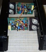
Again Alex has graced and blessed us with an outstanding show of HARD WORK...
In looking over the specifications of the PCB layout program I noticed that it has a built in ability to generate a component side ground plane AUTOMATICALLY.
Could you, WOULD you generate one for the amp board for someone like my self that is interested in such?
Nothing special, what ever it did automatically would suffice for me, I can cut the copper on as need basis.
A NON solid pour would be even greater suited to the job also.
Thanks and AGAIN your skills at PCB layout are PAR EXCELANCE !!!
NAGYS please do the PROTO and give us the OK.
Agree with TAD, kind of getting sidetracked with all the updates and revisions being discussed.
Nothing wrong with the revisions, but I want to try this Goldmund amp. And when the revisions are finalized, I may want to try that amp also.
Agree with TAD, kind of getting sidetracked with all the updates and revisions being discussed.
Nothing wrong with the revisions, but I want to try this Goldmund amp. And when the revisions are finalized, I may want to try that amp also.
Last edited:
To the moderators: Is there any way that I could please edit my very first post? I wold like to add a correction to the schematic and also post additional info. Thanks!
Is this the fastest growing thread ever?
495 posts in 12 day's!
Make that 496
I'm with troyonziess about getting the Goldmund clone finished first before seperate threads break off to make what will be different amplifers.
Respect the time taken by Alex for the pcb design he has done. I can only marvel at such things.
495 posts in 12 day's!
Make that 496
I'm with troyonziess about getting the Goldmund clone finished first before seperate threads break off to make what will be different amplifers.
Respect the time taken by Alex for the pcb design he has done. I can only marvel at such things.
Hello,
I think since Nags started this thread and was gracious enough to provide us with an exact Goldmund schematic we should choose, those who wish, to build the Goldmund clone per the Goldmund specs. No one here would ever discuss making changes and substitutions to a Nelson Pass design or the original Leach amp. Therefore since Alex has done so much superb work we should commence from here. The design works and many were sold at retail to attest to this.
As happens many times on the DIY forum individual personalities and egos begin to get in the way of the original idea. My many years of experience with engineers leads me to believe this wll occur far into the future.
There is a very good pcb layout of the original Goldmund amplifier.
Anyone wish to second this notion. And we can start building.
Tad
Respectfully I disagree with your premise, for 2 reasons.
1. The original PCB layout is not being implemented.
2. The parts used may or may not be the same as the original.
I am not trying inhibit ANYONE from building this amp..
Test it and test it again...
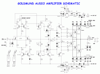
Hi Alex: I've been looking over the schematics all day and have found some mistakes, both in my original schematic and in your .pdf files. Can you please update them so that we all have the correct version. I apologize in advance for the extra work that this will cause.
Alex, in your "Protection Circuit" schematic, .pdf, can you please correct the following:
C4 needs to be reversed in polarity.
C5 needs to be reversed in polarity.
C8 needs to be reversed in polarity.
D4 and D6 should be labeled as 1N4002.
Rel1 should be labeled as JN1A-TMP-DC24V.
L1 should be labeled as 22T MOULDED.
R25 should be labeled as 0.22/3W.
Alex, in your "Goldmund Audio Amplifier" schematic, .pdf, can you please correct the following:
T6(BC182B) is connected wrong/reversed. D1(ZD6V) should connect to the Collector. R12(33K) should connect to the Emitter.
Can you also swap places of C30/C8 and C29/C11? C30 and C29 are small film capacitors (1uF) and they should be shown and connected as close to the input stage as possible.
L1 should be labeled 22T MOULDED in addition to 4uH.
Can you also please label the MOSFETS in parenthesis with the original part numbers (2SK134) and (2SJ49)? This way potential builders will know which transistors were original.
C16 and C35 should be labeled 47uF/100V.
Can you also please add fuses to the schematic? There should be a 10A fuse located between C31 and C32. And also between C34 and C35.
On C8, there's a missing F in the uF.
On C19, there's a missing F in the uF.
Now for the mistake that I made drawing the original schematic. This is an IMPORTANT fix. I'm not sure how hard it will be to implement it into the PCB layout. I apologize Alex. I hope you can fix it easily.
IMPORTANT FIX TO ORIGINAL SCHEMATIC:
The signal point (between Collector of T3 and resistor R1) should be connected to the Base of T8 (NOT to the Base of T7). Also, the signal point (between Collector of T4 and resistor R2) should be connected to the Base of T7 (NOT to the Base of T8).
This is everything that I could find wrong. I'll keep checking and double checking.
What about this one? (see image)
I have made that one a long time ago, I serviced it and still have it. Its JLH's lateral MOS. Very nice.
Attachments
- Home
- Amplifiers
- Solid State
- The Very Best Amplifier I Have Ever Heard!!!!