Thanks for running that sim. Should be workable then. I'll be back in my workshop soon and hope to start this build then. Is there an updated BOM?
There is now an HTML file tree for the SIT3X in the git repository. I suggest you delete any previous downloads from GitHub - lhquam/SIT3X-Power-Amplifier and download and unzip the new contents.
In your browser you can view the file SIT3X-Power-Amplifier.html in the unzipped directory. There are hotlinks to additional HTML files of the tree. All of the previous files should still be there too.
The main updates are to these sections of the HTML tree:
In your browser you can view the file SIT3X-Power-Amplifier.html in the unzipped directory. There are hotlinks to additional HTML files of the tree. All of the previous files should still be there too.
The main updates are to these sections of the HTML tree:
- SIT3X Release/Output Stage
- SIT3X Release/Folded Cascode Front End
Thanks for updating the GitHub, Lynn. I'll have to sort through everything and start getting my Mouser order put together.
The SIT3X X-pot technique for controlling of the modulation of the PFET can also be used with an NFET/PFET combination, rather than requiring a SIT or JFET. I have done some simulations of a minor circuit change to my ZD25 (similar to an XA25) and it is possible to get very low distortion without global feedback. If the ZD25 front end is replaced with the folded cascode front end, then there is no feedback in the FE either.
The only downsides of no global feedback I see are:
Since I built two versions of my ZD25, I am considering modifying one of them for this modification.
- Distortion and residual character changes with Rload, but can be made negative H2 for all loads between 4R and 8R.
- Damping factor is only around 60.
- An output offset servo might be needed.
Below shows an abstract circuit for the modified output stage.
I will probably start a new thread if I pursue this further.
I have the SIT3X PCBs but am now thinking of simply using the Folded Cascode Front End to drive the SissySIT Output stage. Then I don't need the Line Transformers and still end up with a great amp with Zero Global NFB. Rail Voltages will be separate for the two stages.
So my question is what Output Voltage can I expect from the FCFE with the Toshiba devices? Thanks.
My simulations show the following peak output voltages before leaving class-A, using the Toshiba FETs:
- Buffered Folded Cascode: FE rail voltage -11V
- Buffered Current Mirror: FE rail voltage -9V
Thank you Lynn. I will begin with FCFE, rails set to + -43 volts. Not sure if 45 volts is ok. Thanks again.
Building the SIT 3X
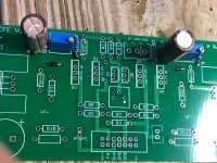
Started to stuff the FCFE boards with the Zener modification.
Cut 3 traces, drilled 4 holes. Didn't have a 150uF/10 volt, so used a larger 220uF/16 volt cap instead. Doesn't fit as well, (hides the R35b and R36b resistors which are put in first) but will do.
I soldered the resistors in first, then installed the new 6.8 volt diode in the new holes I drilled. Wrapped the diode leads around the resistor leads, then soldered.
If you don't solder the resistors in first, you have a wobbly mess to deal with and will have to solder them on both sides of the board as it is hard to flow solder past the diode lead wrap on the bottom.
Next will be the rest of the resistors, diodes, caps and active devises.
Here are photos of each side of the FCFE board.
If I have failed to do the diode mod correctly, please let me know.
Rush
Attachments
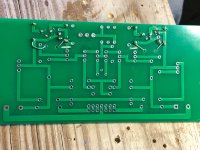
Rush: Your PCB mods look to be correct. 🙂
The larger caps are fine, but eat up space. If the caps are installed first, then the resistors can be made to fit around them.
The larger caps are fine, but eat up space. If the caps are installed first, then the resistors can be made to fit around them.
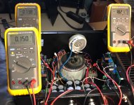
Those pins unused for normal operation. They connect to the FCFE output and ground to easily connect to an oscilloscope or spectrum analyzer. It the shunt on the other side of the ribbon cable connector is removed, the FCFE is detached from the load of the output board, allowing standalone testing of the FCFE board, using an external load resistor and spectrum analyzer.
Thanks a lot for the clarification. And to understand correctly. If I want to set 50 mA on R10 and R11 with the board disconnected from the output board, do I need to connect a load resistor to the FCFE board?
Thank you.
Thank you.
Thanks a lot for the clarification. And to understand correctly. If I want to set 50 mA on R10 and R11 with the board disconnected from the output board, do I need to connect a load resistor to the FCFE board?
Thank you.
For "ordinary" adjustments and use it is not necessary to use the connector pins marked in red or to use any external resistor. The only reason that I added those connector pins was to simplify distortion measurements of the FCFE.
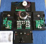
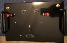
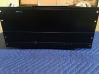
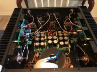
Up and running
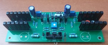
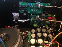
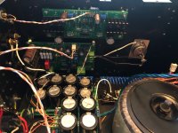
Thank you Lynn for all your help getting my project off the ground.
I am attaching pictures of the build as I went through.
Had a few issues that were mostly due to the lag-time between getting the boards stuffed and finishing the project. Lag-time = short term memory loss!
To start, I am building in a re-purposed Sonance 1250 Amp chassis, reusing the power transformer that has 6 each 29.5Vac-0-29.5Vac secondary windings. Using 3 paralleled windings on each side. The OS boards are configured without the cap multiplier, so a single rail of 0V to -73.5Vdc.
Also using a separate Antek 32Vac 50 VA for the fcfe boards (both sharing the same power supply in dual a rail voltage of +38.5Vdc 0 -38.5Vdc. CRC C=10k uF)
The ground of the fcfe power supply is connected to the 0 rail of the OS power supply. All tricky stuff to keep up with.
One thing is, I installed a 10k resistor where a 100k resistor should go: R23. The OS wouldn't bias up, after finding the mistake everything was good.
Also I forgot to add the jumpers on the back side of the fcfe boards due to time elapsing between doing the diode mod and installing the transistors. That caused some issues that Lynn was able to help track down and fix. But aside from that it all went pretty well.
The amp is biased at 1.65 Amps, 73.5Vdc rail. 120 VA and the heat sinks are hot to touch. About the same as my real First Watt F7.
How does it sound: It is one of the best I have, can't get second opinions right now, due to pandemic. Extended highs, authoritative bass, liquid mids.
I hope to see other builds soon.
Rush
Attachments

Congrats Rush.
Hopefully, my next amplifier design can be simpler. The SIT3X signal path is fairly simple, but the bias circuits add the lots of complexity.
Hopefully, my next amplifier design can be simpler. The SIT3X signal path is fairly simple, but the bias circuits add the lots of complexity.
- Home
- Amplifiers
- Pass Labs
- The SIT-3X Amplifier