The easiest way to obtain lots of positive phase H2 (second harmonic) out of the FCFE is by degenerating the 2SK170 JFET. (This increases negative phase H2 when the signal is inverted for the speaker connections to the output stage).
Attachments
I experimented the past two days with asymmetric degeneration the JFETs in order to change the sned harmonic and determined that any more degeneration than absolutely necessary degraded the sound. The result is to get more negative phase H2, is to only degenerate the 2SK170 (by pot) and not the 2SJ74, as shown in post #682 The SIT-3X Amplifier.
During these experiments, I also found that a 6dB increase in H2 could be obtained with about 4-5 volts increase in the operating point Vds of the SIT.
During these experiments, I also found that a 6dB increase in H2 could be obtained with about 4-5 volts increase in the operating point Vds of the SIT.
Here are plots from the left and right channels of my SIT3X. The OS is biased at 1.8A, with an 8R load, and aan output of 4V peak (1 Watt). The FCFE was adjusted such the the 2nd harmonic of FEOut is minimized. Each plot shows the ratio of H2/H3 in dB vs. the setting of the X pot. The curves are for SIT Vds vaules of 42V, 46V, and 50V. H2 values to the left of the minimum of the plot has negative phase H2, whereas H2 to the right have positive H2 phase.
As you can see, the SITs in the left and right channels have rather different harmonic behaviors.
As you can see, the SITs in the left and right channels have rather different harmonic behaviors.
Attachments
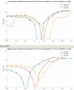
Is the difference between the SIT devices harmonic behaviors because of some measureable thing, like Vgs or the curves are not matched to each other?
Or have you identified a difference in harmonic behaviors we probably can't hear?
Some of this is way over my head.
Got to get a project off my bench, then I will start this one.
Rush
Or have you identified a difference in harmonic behaviors we probably can't hear?
Some of this is way over my head.
Got to get a project off my bench, then I will start this one.
Rush
My guess is that it is a combination of the underlying "primary" triode parameters (mu and Rdrain are all that I consider in my models), and other smaller individual characteristics that shape the Id, Vds, Vgs behavior.
I need to add some more information to those plots: the M1 null point, where the PFET acts as a CCS, and the J1 null point, where J1 acts like a CCS. The H2 null point is already obvious.
In my listening, I find very interesting sonic changes in the vicinity of the M1 null point. At certain X-pot values there is an increased "vibrance" to the sound, for lack of a better term. I am still trying to understand this behavior. Other than being near the M1 null point, nothing in bench measurements explains it.
have anyone finished this project yet?
would anyone share it?
please record and upload to youtube so we can enjoy together 😀
of course not for judging or auditioning, but at least we can understand the results achieved from this project
thanks a lot.
would anyone share it?
please record and upload to youtube so we can enjoy together 😀
of course not for judging or auditioning, but at least we can understand the results achieved from this project
thanks a lot.
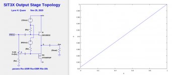
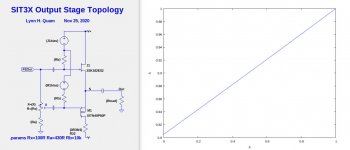
Here are more interesting plots of the SIT3X output stage behavior as a function of operating point Ibias and Vds(J1) and the PFET gate attenuation factor A. A is determined by the voltage divider formed by the Xpot total resistance Rx, the wiper position X, and the resistors Ra, and Rb. The first image shows the output stage topology and a plot showing A as a function of X for my SIT3X build with Rx=100R, Ra=430R, and Rb=10k.
The second image shows plots for the right and left channels at Vds(J1) = 42V, 46V, and 50V. Each plot shows 3 curves:
The second image shows plots for the right and left channels at Vds(J1) = 42V, 46V, and 50V. Each plot shows 3 curves:
- RMS voltage across the PFET sense resistor.
- R22H2 the second harmonic in dB.
- H3 the third harmonic in dB.
Attachments
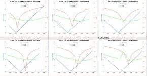
My SIT3X is currently adjusted with Vds=46V for the right channel and Vds=42V for the left channel. During listening for the past month or more, I have found that the sound appears to be most "vibrant", for lack of a better term, near the minima of the V(R22) curves where the PFET acts as a CCS at low signal levels. The choice of Vds values enables for the H2 and H3 levels to be closely matched. I do not understand the cause for this "vibrance", which is to my ears an improvement.
Attachments

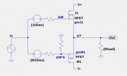
The SIT3X X-pot technique for controlling of the modulation of the PFET can also be used with an NFET/PFET combination, rather than requiring a SIT or JFET. I have done some simulations of a minor circuit change to my ZD25 (similar to an XA25) and it is possible to get very low distortion without global feedback. If the ZD25 front end is replaced with the folded cascode front end, then there is no feedback in the FE either.
The only downsides of no global feedback I see are:
Below shows an abstract circuit for the modified output stage.
I will probably start a new thread if I pursue this further.
The only downsides of no global feedback I see are:
- Distortion and residual character changes with Rload, but can be made negative H2 for all loads between 4R and 8R.
- Damping factor is only around 60.
- An output offset servo might be needed.
Below shows an abstract circuit for the modified output stage.
I will probably start a new thread if I pursue this further.
Attachments
Cascode and current mirrors are somewhat similar, particularly in the case of the Wilson mirror.
A voltage gain of x10 should be perfectly possible with either approach without resorting to feedback. Didn't Nelson show something like this at BAF2013 using LSK devices?
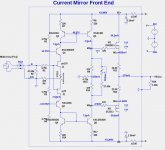
Similar to your suggestion, here is a non-inverting front end using current mirrors. It has about 10X voltage gain and is buffered to drive the capacitive load of the 2SK182ES.
Attachments
Why? That also requires changing 4 other resistors to achieve the desired gain and FET bias current.I would recommend halfing the value of R8 & R17.
Attachments
Yes, that would mean rejigging the bias resistor network.
I have a similar circuit, full Wilson with mirror output cascode; I'm using green LED's for biasing the 2SK2013 & 2SJ313.
Initial listening - it sucked, no bass weight or attack with drum kit - reducing the resistors doubled the mirror output current, solving the MOSFET gate charge issue; now it sounds lovely.
I'm thinking of going back and retrying the cascode mirror with a double summed output.
The JFETS are 8.3mA.
Attachments
That is an interesting result. I have not actually built the current mirror front end, but the FCFE (folded cascode front end) which has the same FET output buffer is very neutral and sounds great driving the SIT3X output stage.
Hi Lynn. On the FCFE with zener mod are the Toshibas still required or could fairchilds be subbed in. I know these were less than ideal previously but am curious if the zener mod makes a difference here. Those Toshibas are getting pretty hard to source.
I haven't tried the Fairchild FETs since my first prototype boards. The primary issue with the Fairchild FETs is the higher Vgs which reduces the maximum voltage swing before clipping by about 3 volts.
I haven't run a simulation with the Fairchild FETs recently, but my estimate is that the resistor values for R8 and R9 must be increased from 470R to about 810R, and R3 might require a small change to preserve the voltage gain of the FCFE.
I haven't run a simulation with the Fairchild FETs recently, but my estimate is that the resistor values for R8 and R9 must be increased from 470R to about 810R, and R3 might require a small change to preserve the voltage gain of the FCFE.
I looked at the FQP3N30 and FQP3P20 datasheets and here are some major differences from the 2SK2013 and 2SJ313 FETs:
- Vgs at 50mA about 2.5V-3.0V higher which reduces voltage swing.
- CCRS at 30V about 3X-4X higher which increases distortion at high frequencies.
- If a separate power supply with higher voltage rails is used for the FCFE, the voltage swing problem is fixed.
- The FCFE distortion is so low that the higher capacitances of the FQP FETs is not a big problem.
- Home
- Amplifiers
- Pass Labs
- The SIT-3X Amplifier