i,m a verified greedy boy like all of us. 😛 I like your take on the SIT bottom but, what is up top with the 182? Oh, and I want the optic mu follower of coarse.
Hiatus, Kits shipments
Just replied today to Soren , and realized that I didn't wrote that "officially" , so:
Do not worry ....
Dunno what's situation with Corona in every particular country , but Serbia is, as majority of Eu, almost totally closed - no flights out and in , so I resume that Post Service isn't exactly functional
Better wait a little , than trying unnecessary ..... somehow I'm calmer if parts are on my shelf than rotting in some Cargo Storage ; in this moment I have 5 shipments to me rotting at Serbian Customs , and 3 on the way to Serbia ..... nobody knows where are they....go figure ......
Hiatus
stay well and be safe!
Same ..mah Korg is being attacked by corona in the immigration warehouse ..
Stay stronk my korgie.
Stay stronk my korgie.
Did you receive my PM ?
yup
got to sleep in the morning, but then I did my proper stint
sometimes as Tesla, sometimes as Don Juan Matus
I'm glad you got the PM.
I know what it's like to wake up as Tesla...
One can't write down the ideas fast enough.
Thanks for reminding me to put on a pot of coffee.
G
I know what it's like to wake up as Tesla...
One can't write down the ideas fast enough.
Thanks for reminding me to put on a pot of coffee.
G
Last edited:
As there is a lull in activity, I have a couple of questions:
1 - What type/kind of power supply is needed for the bias part of the circuit?
2 - Is there any difference/improvement in using 2SK170BL FET's, versus the SMD version supplied in the kits? I'm confident I can REMOVE a SMD, not sure I could ADD an SMD, which is why I was so glad you are supplying them on the PCB's.
3 - Do you recommend snubbers on the transformer rail to prevent ringing?
1. written on each schematic of lower/gain portion , lower right corner ;
in case of SIT - 15Vac/100mA means that you need xformer like that , one xformer
can cover both channels;
in case of Schade - 30Vct (AC)/100mA means that you need xformer like that , one
xformer can cover both channels;
2.I expect them (both iteration) having job easy enough , so you'll hardly hear any
difference; though - if you are scarce with T092 JFets, having tiny critters presoldered on
pcb can save these for some other use
3.Quasimodo time, no doubt - and that time is always well spent
Between Tesla readings and info on Don Juan I will stay busy 😀
Haven't read Castaneda books for years.
Also revisiting the greatness of Tesla.
Maybe something will rub off🙄
don juan matus - Bing video
Thanks ZM
Haven't read Castaneda books for years.
Also revisiting the greatness of Tesla.
Maybe something will rub off🙄
don juan matus - Bing video
Thanks ZM
Does the 15 vac P/S need to be regulated? Linear?
elwood , that's data for small xformer , AC means Alternating Current ; rectifier and regulation are on board
Between Tesla readings and info on Don Juan I will stay busy 😀
Haven't read Castaneda books for years.
Also revisiting the greatness of Tesla.
Maybe something will rub off🙄
don juan matus - Bing video
Thanks ZM
if you need Castaneda's e-books , just buzz
ZM at his finest:
I am very late in learning about this thread and see lots of good stuff here.
As many of you know I have been working with the 2SK182ES, making many measurements of the devices, testing them in the mu-follower circuit, mathematically analyzing the mu-follower, and actually building a "muscular" SIT amplifier similar to the Singing Bush.
SIT measurements, Mu Follower, and amplifier build
I have some questions, comments, and suggestions.
- Regarding the circuit in post #5 (the peasant half), how is the voltage stabilized ad the node A' between the mu-follower and the IXYS M1 drain? The transformer feedback is AC only, thus it seems that node A' could wander around a lot without some sort of DC feedback.
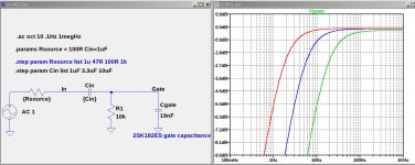
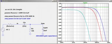
- In post #133 The Singing Bush there was a question about the inp(ut coupling capacitor. My measurements of the 2SK182ES show about 19nF input capacitance of the device, and that capacitance is non-linear. The input and gate capacitors together will become a voltage divider. The bigger the input capacitor, the less distortion due to the non-linearity of the gate capacitance. The input capacitance together with the gate bias voltage resistor (10k?) determine the low frequency rolloff. I will show a simple schematic.
Last edited:
yo my lhquam man 🙂
1. I didn't play smart one here, what I did - started with Pa's concept from BAF 2015 lecture and tried to build (whatever small I could) from that ...... and as you can see , there is no DC feedback at all, entire shebang relying on nice TempCo of chosen pucks ; pretty much everything is already shown and explained with some textual data here and there, at least what I was able to realize as being important to write down
conclusion - there is no significant difference between cold and hot ( temp equilibrium) state - neither in Iq nor in voltage potential at output node (or lower drain voltage, whatever), with biasing mechanism used here
2.in post #133 Soundhappy did comment on input cap before input buffer ( and I did cover reply to him in #131 - 1uF is plenty for Rin of 100K) ; there is no capacitor in between input buffer and SIT gate, deliberately - because my goal was to fight with hungry and hysterical SIT gate with brute force - both DC connection and as much Cojones I could squeeze in , without breaking a bank or sacrificing SQ (or level of wakooness, if you like)
Freq. response graphs and graphs showing level of fundamentals in function of frequency.... are making me green ..... so , I resume that issue is covered.... in any case, best I could do it
1. I didn't play smart one here, what I did - started with Pa's concept from BAF 2015 lecture and tried to build (whatever small I could) from that ...... and as you can see , there is no DC feedback at all, entire shebang relying on nice TempCo of chosen pucks ; pretty much everything is already shown and explained with some textual data here and there, at least what I was able to realize as being important to write down
conclusion - there is no significant difference between cold and hot ( temp equilibrium) state - neither in Iq nor in voltage potential at output node (or lower drain voltage, whatever), with biasing mechanism used here
2.in post #133 Soundhappy did comment on input cap before input buffer ( and I did cover reply to him in #131 - 1uF is plenty for Rin of 100K) ; there is no capacitor in between input buffer and SIT gate, deliberately - because my goal was to fight with hungry and hysterical SIT gate with brute force - both DC connection and as much Cojones I could squeeze in , without breaking a bank or sacrificing SQ (or level of wakooness, if you like)
Freq. response graphs and graphs showing level of fundamentals in function of frequency.... are making me green
..... so , I resume that issue is covered.... in any case, best I could do it
Last edited:
As promised, here LTSpice simulations of the RC circuit characteristics.
The first circuit show the low frequency-off for different values of the coupling capacitor, assuming a 10K resistor to the bias voltage generator.
The 2nd circuit shows the high frequency roll-off for difference values of the input source resistance.
The first circuit show the low frequency-off for different values of the coupling capacitor, assuming a 10K resistor to the bias voltage generator.
The 2nd circuit shows the high frequency roll-off for difference values of the input source resistance.
Attachments
Yes, the best place for the input capacitor (if needed) is before the JFETs.
Alternatively, in the circuit of post #5 (peasant half) is it possible eliminate R4 and P1, and then perform the bias offset at the JFET gates. The lowers the output impedance of the buffer.
Alternatively, in the circuit of post #5 (peasant half) is it possible eliminate R4 and P1, and then perform the bias offset at the JFET gates. The lowers the output impedance of the buffer.
'twas a choice of leaving in input cap or going DC couple all the way
I chose this way as better overall
I chose this way as better overall
- Home
- Amplifiers
- Pass Labs
- The Singing Bush