I was just hoping to make some pocket money with my own PCB design, maybe I'm just too slow for this. I am going to work on the Salas regs and then I will tweak everything to fit together on the PCB.
Haha, no worries, few would be interested in SMD boards, and yours will attract a lot by offering all-in-1 solution in one assembly saving a lot of hassle dealing with individual cell units, as Jean Paul pointed out. I for one will be very interested in your design.
I have some ideas but I really appreciate the guidance and inspiration from you, Jean and others.
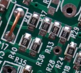
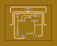
Looks R3 & C2 are mounted end to end.
The gap between the two is very narrow, too narrow to get a soldering tip in there.
The first smd to be soldered will be easy., but after it is in place the second will be difficult to solder since you cannot get in to heat the solder pad.
There are others where access to the solder pad is very narrow
Last edited:
Looks R3 & C2 are mounted end to end.
The gap between the two is very narrow, too narrow to get a soldering tip in there.
The first smd to be soldered will be easy., but after it is in place the second will be difficult to solder since you cannot get in to heat the solder pad.
There are others where access to the solder pad is very narrow
Hi Andrew, thanks for the comment and the concern.
I guess you did not realize the 0805 decal I'm using has enlarged land specifically designed for hand soldering. The narrowest end-to-end in my layout is 0.64mm between R12 and R13. I could reduce that to 0.25mm by placing the component even closer and there is still not a problem soldering parts by hand. The attached picture is from my other project hopefully it explains better. The narrowest spot in that picture is 0.65mm.
Attachments
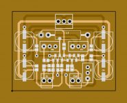
Congratulations!This is my attempted layout using SMD dual transistors, that wont likely go obsolete any time soon. SMD Rs and Cs are 0805 size, quite easy to handle, and a perfect starter size. The 0805 soldering land in this layout has slightly longer pads and was specifically designed for easy hand soldering.
That is.
Go ahead!
That pic shows lots of end to end clearance to get a soldering iron in.
The PCB layout misled me into thinking they were much closer together.
I have bought a few Group Buy PCBs where the layout designer got this quite wrong.
The PCB layout misled me into thinking they were much closer together.
I have bought a few Group Buy PCBs where the layout designer got this quite wrong.
This will be absolutely right . In any case It is your work.I was just hoping to make some pocket money with my own PCB design, maybe I'm just too slow for this. I am going to work on the Salas regs and then I will tweak everything to fit together on the PCB.
I was told that the DCB1 can swing rail to rail, and that some users apparently need this functionality? Who needs a 20Vpp buffer for their equipment, and what equipment?
I was told that the DCB1 can swing rail to rail, and that some users apparently need this functionality? Who needs a 20Vpp buffer for their equipment, and what equipment?
F4 ? 😀
20 Vpp seems nonsense (and very non standard). You can not accomodate for everybodies needs as well. Just focus on the goal of a finished product with the necessary bells and whistles to function properly in 99% of cases. Take real life situations into account i.e. sources that may carry DC, power amps that may be sensitive to DC, power on/off muting, RF noise (input filter), power supply RF decoupling, readily available parts, standard transformers with good specs like small stray field etc etc. Your kuartlotron is only one Lego piece in a total design. Please change view to a total design that is easy to replicate in various countries in the world so 115V/230V capable etc.
It is very hard if not impossible to make everybody happy and making it a democratic process will only hamper you and it may cause the project to be a never ending story. Just write down your design goals first and design the PCB accordingly, test it and make it a GB. If you want to make everybody happy then chances are likely that you end up an unhappy person 😀 Take this from a guy that already made those mistakes, check my projects and GBs here... Same mistake over and over again: showing stuff and then folks start to expect things. Better work on it continuously and present a complete board when it is ready.
Just some tips, maybe a bit direct but that is our style here 🙂
Nattawa made a very nice design (IMO the best till now), I would not hesitate and make that one a stereo version (why design mono boards at all with all masochistic wirng and stuff ?) as it is compact. I would add SMD pads for the 470 uF decoupling caps too. TH days are nearly over, alas. TO92 transistors will be 2015's tubes 😉
Last edited:
No.I was told that the DCB1 can swing rail to rail, and that some users apparently need this functionality? Who needs a 20Vpp buffer for their equipment, and what equipment?
The B1 and DCB1 are simply fet followers that are loaded/biased with a fet CCS.
They inherently develop massive 2nd harmonic as supply rail is approached.
A sensible lowish distortion maximum output would be around half the supply rails, i.e 10Vpp = 5Vpk = 3.54Vac
The usual CDP output of 2Vac to 2.2Vac would leave sufficient headroom (of ~10dB) to avoid most of the increased distortion at maximum levels.
I was actually once using the Kuartlotron to drive a Lfet output stage with my sensitive speakers. I think I'll just count that as good enough.
In the diagram of nattawa (post # 434) there is a 4.7 uF capacitor on the input. This capacitor is't really an advantage?
It depends on what it is connected to. If it is connected to a switch, then you might add a DC blocking capacitor in series with the switch to prevent snaps when the switch is turned.
If a few mV of offset is a problem for your destination, then you will want to add a DC blocking cap on the output.
Equipment that is not DC coupled however will have it's own input capacitor, so adding one to the buffer should not be necessary.
If a few mV of offset is a problem for your destination, then you will want to add a DC blocking cap on the output.
Equipment that is not DC coupled however will have it's own input capacitor, so adding one to the buffer should not be necessary.
Adding the pads for input/output caps caters for everyones needs. It is the builders responsibility to check his/hers situation and use caps wherever they are needed. So adding pads with 2.5 or 5 mm distance between the caps pads is efficient for DC coupled purposes. No caps needed ? Then just use jumper wires.
Just an example: more than once I experienced CD players to have a large offset voltage at the outputs but only when muted. This was perfectly visible when looking at the woofers in my DC coupled chain of then (Akai AM-U5....one of the first commercial DC coupled open loop amplifiers and a good one too). I learned to appreciate the virtues of DC blocking caps and ALWAYS use those at the inputs of power amps to protect the investment (so my buffers/preamps are DC coupled at the outputs). Problems arise when some sources already have output caps and others who don't....2 caps in series is not the best recipe. Careful planning of the complete chain is a necessity. Manufacturers very often play safe and use output caps in their CD players, tuners etc. and they use input caps at the power amps as they don't know what the user will connect.
Just an example: more than once I experienced CD players to have a large offset voltage at the outputs but only when muted. This was perfectly visible when looking at the woofers in my DC coupled chain of then (Akai AM-U5....one of the first commercial DC coupled open loop amplifiers and a good one too). I learned to appreciate the virtues of DC blocking caps and ALWAYS use those at the inputs of power amps to protect the investment (so my buffers/preamps are DC coupled at the outputs). Problems arise when some sources already have output caps and others who don't....2 caps in series is not the best recipe. Careful planning of the complete chain is a necessity. Manufacturers very often play safe and use output caps in their CD players, tuners etc. and they use input caps at the power amps as they don't know what the user will connect.
Attachments

Last edited:
Power on off muting I like to use a normally closed ssr to ground. Just a suggestion as you can zener power it so it only powers on at near full psu power and powers down quickly as well. CPC1219 is about $.80. I like to run the zener from rail to rail so if one rail fails the circuit mutes.
Mmm, a non linear part for muting a small signal buffer while a relay with just contacts can do the job fine ? Never used SSRs for that purpose...interesting though.
Last edited:
The linearity doesnt matter. Use it to ground. A relay works too but this is more reliable, cheaper and cooler. Specs say 16ohms but in reality its about 7.
I was told that the DCB1 can swing rail to rail, and that some users apparently need this functionality? Who needs a 20Vpp buffer for their equipment, and what equipment?
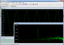
I don't have really low THD gen that swings that high so I used the simulator. Suggests it can hold very well up to +/- 9.5V signal when on +/-10V rails. With such swing 1kHz signal at +16dB it predicts 2nd H at -74dB i.e 90dB down. 3rd H at -64dB i.e. 80dB down.
Some specific DIY Pass or few other very low sens amps may use that.
Attachments
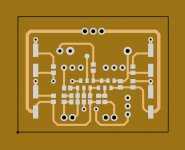
Hello everyone!
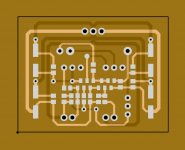
I 've never worked with SMD components but I'll try to see if my first test works. I designed a layout for Kuartlotron with BC850 and BC860.
If you think I'm going straight into the wall, tell it! 😀
Regard's!
I 've never worked with SMD components but I'll try to see if my first test works. I designed a layout for Kuartlotron with BC850 and BC860.
If you think I'm going straight into the wall, tell it! 😀
Regard's!
Attachments
- Home
- Source & Line
- Analog Line Level
- The Kuartlotron - keantoken's simple error-correction superbuffer