Re: Mark's post. Hmmm, I had forgotten about these bench supplies. Almost cheaper to buy one of these than build one, for M2X use, no? Certainly easier that the acquire and build of the usual PS. I like the low ripple, too.
I recall a fellow on this list using two switching units to provide the split voltages, together with some outboard capacitance to make a go of it, reporting excellent results.
That case was instructive, too.
Remarkable.
I recall a fellow on this list using two switching units to provide the split voltages, together with some outboard capacitance to make a go of it, reporting excellent results.
That case was instructive, too.
Remarkable.
Yikes! I attached the wrong link to post #3859. Very sorry! Here is the one I should have provided
30 Volt Tri Output Linear DC Power Supply 3.0 Amps
Thanks to eagle-eyed member 6L6 for noticing the error first.
30 Volt Tri Output Linear DC Power Supply 3.0 Amps
Thanks to eagle-eyed member 6L6 for noticing the error first.
2 halogen light used toroidals 12V a bridge and some caps are far cheaper than those variable PSUs...
Yikes! I attached the wrong link to post #3859. Very sorry! Here is the one I should have provided
30 Volt Tri Output Linear DC Power Supply 3.0 Amps
Thanks to eagle-eyed member 6L6 for noticing the error first.
Or if you want 5 amps current for only $4 more, just buy 2 of these:
30 Volt Adjustable Linear DC Power Supply, 5 Amps
They used to make a dual 5A but it was discontinued.
I give the backside of high power semiconductors a couple of very light swipes across a flat diamond whetstone, before mounting them. It reassures me that I did everything possible to get rid of burrs and spikes on the mounting surface, which might damage the insulator pad.
Here is an example (link)
Mark,
thanks for this link. Just ordered it. And Amazon will deliver it tomorrow. That is just a little scary. I guess based on past purchases they were ready for me and had already staged it here in Tucson.
First, I connected with the bulb, then without. Of course there was to be heresy and there was a mistake. I don't know where I got 37R4 instead of 37k4. After the exchang offset was set ~0. On the R channel I have 0.65V through r13 and r14 on L 0.61V. What could be the reason? Over half an hour of operation and temperature at Q1 60 ° CIf you do all three of these actions before powering up an M2x amp channel card
- completely remove the input stage daughter card
- short the IPS daughter card input (bolt #2) to the IPS daughter card output (bolt #4) with many figure-eight wraps of copper wire
- insert a shorting plug into the RCA input jack, which connects INPUTSIGNAL to GROUND
then you won't force destructive amounts of DC into the Edcor transformer's primary coils.
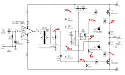
I strongly recommend that you use your DVM, in "continuity tester" mode, to become absolutely convinced that you've correctly identified bolt 2 and bolt 4. Studying the schematic of the amp card (mother board) below, you can see that only one of the four bolts has electrical continuity to capacitor C0. Eureka and congratulations, you have found bolt #2! Now devise a similar plan to identify bolt #4.
_
View attachment 895051
Once moreFirst, I connected with the bulb, then without. Of course there was to be heresy and there was a mistake. I don't know where I got 37R4 instead of 37k4. After the exchang offset was set ~0. On the R channel I have 0.65V through r13 and r14 on L 0.61V. What could be the reason? Over half an hour of operation and temperature at Q1 60 ° C
View attachment 895051

Can you explain to me what the letters aa, bb etc. mean?My browsers (Chrome, Firefox) can't display the image embedded in post #3867.
In case it happened to be a schematic of the M2x amplifier channel board, I've attached another of those below.
_
I attach Node Names to individual nodes of the circuit schematic, in order to reduce or eliminate ambiguity.
For example, the voltage dropped across R10 is measured by connecting one DVM probe to node DD and the other DVM probe to node EE. It's easy to communicate this using node names.
You can compare the voltage dropped across R10, to the voltage dropped across R12, [one probe on KK, the other on KK] and also to the voltage dropped across R11 [one probe on node MM, the other no node KK]. Check whether their voltage drops are sensible and reasonable.
In normal operation of the optoisolator biasing control system, current flows from DD to EE to MM to KK to JJ.
Since R10 and R12 are both 100 ohms, and since in normal operation they carry the same current, we expect that the voltage drop across R10 is exactly equal to the voltage drop across R12. But if the board is soldered incorrectly, or if R10 and R12 are not actually equal (stuffing error?), then the voltage drop across R10 won't be equal to the voltage drop across R12. So that's a useful experiment to perform.
Since R11 is 2.21 times larger than R10, and since in normal operation they carry the same current, we expect that the voltage drop across R11 is exactly 2.21 times larger than the voltage drop across R10. If they are not it suggests some kind of error in that vicinity, so this would be another useful experiment to perform.
You could save yourself some time by writing out a pair of tables; one for the channel that you feel is working correctly, and another table for the channel that you feel is not working correctly. Then you could tabulate your measured voltage drops for each channel
and notice all of the places where there are significant differences between the two channels.
_
For example, the voltage dropped across R10 is measured by connecting one DVM probe to node DD and the other DVM probe to node EE. It's easy to communicate this using node names.
You can compare the voltage dropped across R10, to the voltage dropped across R12, [one probe on KK, the other on KK] and also to the voltage dropped across R11 [one probe on node MM, the other no node KK]. Check whether their voltage drops are sensible and reasonable.
In normal operation of the optoisolator biasing control system, current flows from DD to EE to MM to KK to JJ.
Since R10 and R12 are both 100 ohms, and since in normal operation they carry the same current, we expect that the voltage drop across R10 is exactly equal to the voltage drop across R12. But if the board is soldered incorrectly, or if R10 and R12 are not actually equal (stuffing error?), then the voltage drop across R10 won't be equal to the voltage drop across R12. So that's a useful experiment to perform.
Since R11 is 2.21 times larger than R10, and since in normal operation they carry the same current, we expect that the voltage drop across R11 is exactly 2.21 times larger than the voltage drop across R10. If they are not it suggests some kind of error in that vicinity, so this would be another useful experiment to perform.
You could save yourself some time by writing out a pair of tables; one for the channel that you feel is working correctly, and another table for the channel that you feel is not working correctly. Then you could tabulate your measured voltage drops for each channel
- V(DD , OUT)
- V(DD , EE)
- V(EE , MM)
- V(MM , KK)
- V(KK , JJ)
- V(OUT , JJ)
and notice all of the places where there are significant differences between the two channels.
_
Last edited:
I checked some of the points indicated and there are no significant differences.
DD-EE 45.8 / 46.6mV
EE-MM 1.034 / 1.035V
MM-KK 98 / 100mV
KK-JJ 44.8 / 45.4mV
Offset 0 / 6mV At the moment, I checked the bias and I have 0.61V on both channels through 0.47R resistors. I already know why there was such a difference - a mistake on r6. I did not check it after replacing the resistor. Thank you for your help.
Here's how I did it and the parts from Amazon:
https://www.amazon.com/Cal-Hawk-AZG...NW9&pd_rd_i=B002X4AFL0&ref_=pd_bap_d_rp_1_1_t
What is that goop you put everywhere?
I mailed Edcore about shipping to Sweden on the two 22$ transformers.
154$was the answer,this, it is the only way to get the transformers over seas...
No thank you was my answer...🙁
154$was the answer,this, it is the only way to get the transformers over seas...
No thank you was my answer...🙁

I'll second Mark on Don Audio as a European source for the Edcors; I have bought several times from them.
They do have the little Edcors in stock, as well.
Best regards,
Claas
They do have the little Edcors in stock, as well.
Best regards,
Claas
Hi all!
Question for IPS6 Rev A. image on Post #4
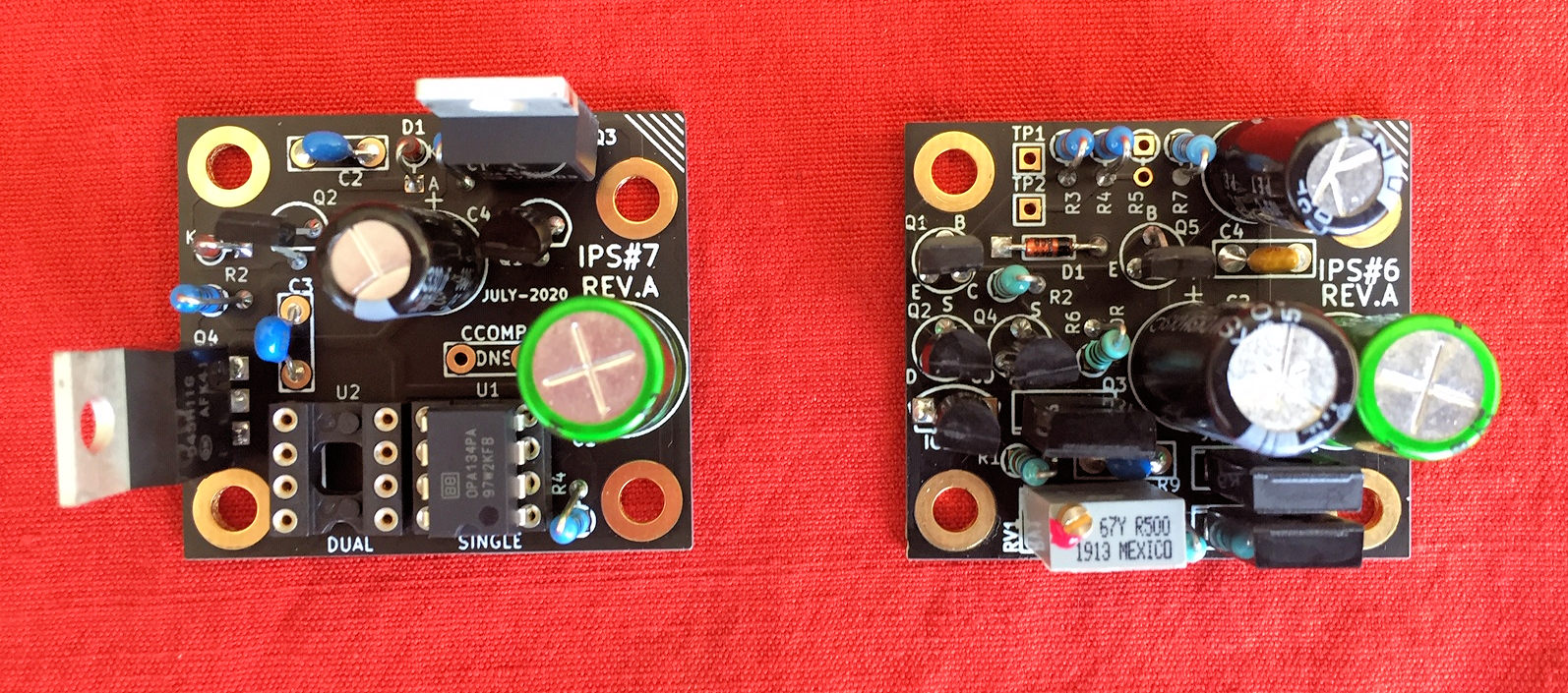
Q2 and Q4 (J113) data sheet shows pin config for TO-92 case
https://www.mouser.com/datasheet/2/308/MMBFJ113_D-1811481.pdf
Looking at the image, is the orientation of the J113 on the pic with respect to the print on the pcb (D-S-G clockwise) and pin assignment correct or I am mistaken?
Thank you!
Abe
Question for IPS6 Rev A. image on Post #4
Q2 and Q4 (J113) data sheet shows pin config for TO-92 case
https://www.mouser.com/datasheet/2/308/MMBFJ113_D-1811481.pdf
Looking at the image, is the orientation of the J113 on the pic with respect to the print on the pcb (D-S-G clockwise) and pin assignment correct or I am mistaken?
Thank you!
Abe
You have it right... Just put them in like the PCB indicates with the middle (source) going to the source designation of the PCB and you will have it right.
The drawing they have makes it look wrong as in the gate and drain are reversed. Just follow the match the PCB and transistor flat with center to source and it will be correct.
The drawing they have makes it look wrong as in the gate and drain are reversed. Just follow the match the PCB and transistor flat with center to source and it will be correct.
Last edited:
You have it right... Just put them in like the PCB indicates with the middle (source) going to the source designation of the PCB and you will have it right.
The drawing they have makes it look wrong as in the gate and drain are reversed. Just follow the match the PCB and transistor flat with center to source and it will be correct.
Thank you!
Abe
No problem... don't be afraid to bust out your meter and check to see what is what. There are some great videos out there which can help you through it... when in doubt, you can always check it this way... you can also look at the schematic and test that as well.
Trust, but verify! 😀
JT
Trust, but verify! 😀
JT
- Home
- Amplifiers
- Pass Labs
- The diyAudio First Watt M2x