... hi again. I think this was a little unclear so a clarification:
What I meant to say was that the DSD NoDAC itself has a 50 kHz RC filter AND the AD7760 EVB has a 19 MHz filter. I should have checked this earlier on - didn't think about it ... but given that it is this high up in frequency (and a first order filter), and DSD256 is 11.2 MHz Fs wouldn't it be reasonable to assume that the ADC is not really affected by a signal at this frequency?
@Marcel : If I post a couple of screendumps of what the spectrum looks like at DSD128 and DSD256 can you then see if there is any ADC aliasing - or the like?
Cheers, Jesper
This morning I have checked the input of the AD7760 EVB and besides the ~ 50 kHz filter I have it has a filter at 19 MHz (they call it the first aliasing point).
What I meant to say was that the DSD NoDAC itself has a 50 kHz RC filter AND the AD7760 EVB has a 19 MHz filter. I should have checked this earlier on - didn't think about it ... but given that it is this high up in frequency (and a first order filter), and DSD256 is 11.2 MHz Fs wouldn't it be reasonable to assume that the ADC is not really affected by a signal at this frequency?
@Marcel : If I post a couple of screendumps of what the spectrum looks like at DSD128 and DSD256 can you then see if there is any ADC aliasing - or the like?
Cheers, Jesper
@Marcel : If I post a couple of screendumps of what the spectrum looks like at DSD128 and DSD256 can you then see if there is any ADC aliasing - or the like?
Cheers, Jesper
Probably not. Your 7 kHz experiment could be interesting, assuming you can keep the connections to the capacitors very short (otherwise the wire inductance may limit the filtering at 11 MHz too much).
Based on the circuit diagram of #2280, it appears that there is only one tap. In this case, the issue might not be switching noise but rather overshoot or undershoot, based on my experience. When using high-speed components, the rise and fall times tend to be nearly equal, but overshoot can increase, causing measured values to worsen.
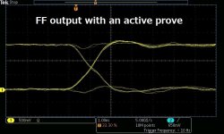
I drive the current switch with FPGA flip-flops. However, using the fastest buffer (24mA) doesn't have good results. It's often better to use a slower buffer of around 6mA for improved outcomes. See pic.1 for the output waveform. At 24mA, the rise time is around 1nsec, but the overshoot is significant, leading to unfavorable results.
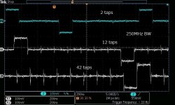
With a single tap, I believe the THD limit is around -100dB. While SNR would be optimal since the overall level is relatively small, surpassing 100dB is challenging. Increasing taps improves THD and SNR, yet differences in tap characteristics impose limitations. Pic.2 illustrates the output waveform as taps are increased. This is for zero input, resulting in a change of about 100mV near 0 volts. 100mV means one tap voltage.
Components like 74AC74, having only one GND, can experience increased noise and overshoot when switching at high speeds. Despite properly bypassing the power supply on a four-layer board, degradation likely occurs due to increased noise and overshoot. Components with multiple GND connections might lead to varying degrees of degradation.
I drive the current switch with FPGA flip-flops. However, using the fastest buffer (24mA) doesn't have good results. It's often better to use a slower buffer of around 6mA for improved outcomes. See pic.1 for the output waveform. At 24mA, the rise time is around 1nsec, but the overshoot is significant, leading to unfavorable results.
With a single tap, I believe the THD limit is around -100dB. While SNR would be optimal since the overall level is relatively small, surpassing 100dB is challenging. Increasing taps improves THD and SNR, yet differences in tap characteristics impose limitations. Pic.2 illustrates the output waveform as taps are increased. This is for zero input, resulting in a change of about 100mV near 0 volts. 100mV means one tap voltage.
Components like 74AC74, having only one GND, can experience increased noise and overshoot when switching at high speeds. Despite properly bypassing the power supply on a four-layer board, degradation likely occurs due to increased noise and overshoot. Components with multiple GND connections might lead to varying degrees of degradation.
Attachments
Hi Marcel & xx3stksm,
@Marcel : I will try out filtering at appr. 7 kHz and see what happens. Thanks again for following up 😉
@xx3stksm : Thank you also for commenting and your pictures. Just FYI regarding a single tap I can reach appr. - 107 dB THD with the NC7SZ74 FF at DSD128 with a high FF VDD. The - 107 dB THD is as measured with my AD7760 EVB - and on a good day for HQPlayer (as the distortion level in my experience varies with HQPlayer).
I think your thoughts about over- & undershoot (O&U onwards ;-)) is really interesting. However, do you think that O&U is a realistic explanation when going from DSD128 to DSD256? It is only a ~ 6 MHz difference and the distortion difference is ~26 dB. Then again ... GND pin impedance & VDD pin impedance would both double - and then if the IC somehow is also a bit non-linear wrt frequency, then maybe .. ??
I am wondering if there may be a way to reduce this O&U while still keeping a low phase noise? All of these FFs: the 74AUP1G74, the NC7SZ74 and likely (I don't know) the 74AUC1G74 are low phase noise devices so I reckon that it would be feasible to try to reduce the O&U, if possible while still using these FFs ... ? If using slower FFs the phase noise likely will increase and the rise/fall times may no longer be identical (right?).
Maybe adding resistors to either the GND pin or the VDD pin may reduce O&U? Might you have any thoughts on this?
Cheers, Jesper
I am using a current switch, allowing for switching at voltages as low as around 0.7V. The FPGA buffer can handle voltages from 3.3V to 1.2V, so for high-speed switching, 24mA at 3.3V would be ideal. However, upon experimentation, it turns out that 6mA at 1.2V is the optimal setting. The reason behind this is that switching with high voltage and current can destabilize the ground, leading to undesirable effects. A larger overshoot worsens characteristics, and it's possible that the reference voltage is affected.
However, at 1.2V and 6mA, there is a slight difference between rise and fall times, which is adjusted by altering the phase of the internal PLL of FPGA. This adjustment is quite sensitive, requiring a precision of about 0.1ns, which is the limit of Spartan6. If, for instance, there's an error of 1ns here, it translates to 1ns out of approximately 160ns for DSD128 and 80ns for DSD256. Considering the frequency doubling, the impact could be at least four times greater.
In the case of the monolithic AK4499eq, there is minimal degradation even at DSD256. It seems that the switching error is smaller compared to discrete components. With FPGA, given the numerous power pins, it exhibits resistance to simultaneous switching, but at DSD256, overall noise levels apparently rise. Despite adjustments, finding the optimal values remains challenging.
For components like NC7SZ74, rise and fall times tend to depend on the component, so using the maximum power supply voltage would be better. Increasing taps might be difficult to adjust for varying component characteristics, so using a single tap could be a better choice. In cases where FPGA is not involved, using components with multiple GND pins on a four-layer board seems like a good approach.
Rege
So it's better AK4499eq than FPGA?
I always suspected upsampling to higher rates poluted more the power rails.
I always suspected upsampling to higher rates poluted more the power rails.
@xx3stksm : Once again thanks for your helpful feedback 👍 ... A few comments:
Hmmm ... with reference to #2280 and the attached screendump of Marcel's layout for the RTZ FIRDAC the GND path I have used for my NoDAC layout is "direct" if I can call it so. That is the decoupling capacitor's GND pad is connected directly to GND which is then led to the NC7SZ74's GND pin through the GND fill. On the other hand Marcel connects the decoupling capacitors' GNDs to GND near the capacitor and then leads the GND from these capacitors to the GND pin (pls see attachment). In my understanding this would lead to higher ground bounce but as I understand Marcel some of his "colleagues" (?) have found this to work better (I can't remember the reason why). And the RTZ FIRDAC performs outstandingly (in case you would like to see (& have not seen) the latest results here is a link):
https://www.diyaudio.com/community/...t-register-firdac.379406/page-55#post-7419240
So maybe there would be an idea in leading the decoupling capacitor's GND directly to the GND pin on the NC7SZ74 - thus referencing Q and Qnot & the FF's own GND pin return currents to the capacitor's GND? Tricky this is
The tinylogic series, of which the NC7SZ74 is a part of, also includes a single-ended FF - the NC7SZ374. Do you think it would make sense to split the Q and Qnot outputs e.g. with two NC7SZ374s - and then adjust the timing to each of these single-ended FFs ever so slightly with the series resistors feeding each of the CLK pins of the 374s? It would allow for some adjustment of synchronicity between the two FFs, although it wouldn't allow for adjustment of rise/fall times ...
The only one I know of with more center GNDs is the 74AC11478 but it appears to be unobtainable in practice ...
Cheers, Jesper
The reason behind this is that switching with high voltage and current can destabilize the ground, leading to undesirable effects. A larger overshoot worsens characteristics, and it's possible that the reference voltage is affected.
Hmmm ... with reference to #2280 and the attached screendump of Marcel's layout for the RTZ FIRDAC the GND path I have used for my NoDAC layout is "direct" if I can call it so. That is the decoupling capacitor's GND pad is connected directly to GND which is then led to the NC7SZ74's GND pin through the GND fill. On the other hand Marcel connects the decoupling capacitors' GNDs to GND near the capacitor and then leads the GND from these capacitors to the GND pin (pls see attachment). In my understanding this would lead to higher ground bounce but as I understand Marcel some of his "colleagues" (?) have found this to work better (I can't remember the reason why). And the RTZ FIRDAC performs outstandingly (in case you would like to see (& have not seen) the latest results here is a link):
https://www.diyaudio.com/community/...t-register-firdac.379406/page-55#post-7419240
So maybe there would be an idea in leading the decoupling capacitor's GND directly to the GND pin on the NC7SZ74 - thus referencing Q and Qnot & the FF's own GND pin return currents to the capacitor's GND? Tricky this is
However, at 1.2V and 6mA, there is a slight difference between rise and fall times, which is adjusted by altering the phase of the internal PLL of FPGA.
The tinylogic series, of which the NC7SZ74 is a part of, also includes a single-ended FF - the NC7SZ374. Do you think it would make sense to split the Q and Qnot outputs e.g. with two NC7SZ374s - and then adjust the timing to each of these single-ended FFs ever so slightly with the series resistors feeding each of the CLK pins of the 374s? It would allow for some adjustment of synchronicity between the two FFs, although it wouldn't allow for adjustment of rise/fall times ...
using components with multiple GND pins on a four-layer board seems like a good approach.
The only one I know of with more center GNDs is the 74AC11478 but it appears to be unobtainable in practice ...
Cheers, Jesper
Attachments
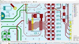
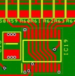
Those results are from my board which has slightly different layout than Marcel's. I use GND planes (layers 2 & 4) so FF decoupling capacitor as well as FF GND pin are connected to GND planes with vias only.Hmmm ... with reference to #2280 and the attached screendump of Marcel's layout for the RTZ FIRDAC the GND path I have used for my NoDAC layout is "direct" if I can call it so. That is the decoupling capacitor's GND pad is connected directly to GND which is then led to the NC7SZ74's GND pin through the GND fill. On the other hand Marcel connects the decoupling capacitors' GNDs to GND near the capacitor and then leads the GND from these capacitors to the GND pin (pls see attachment). In my understanding this would lead to higher ground bounce but as I understand Marcel some of his "colleagues" (?) have found this to work better (I can't remember the reason why). And the RTZ FIRDAC performs outstandingly (in case you would like to see (& have not seen) the latest results here is a link):
https://www.diyaudio.com/community/...t-register-firdac.379406/page-55#post-7419240
Attachments

@bohrok2610 : thanks for sharing! BTW I did not mean to imply that it was Marcel's layout ... I thought it was apparent in the thread post that it was basically Marcel's circuitry design but your layout (and some changes). But hereby corrected 😉
Cheers, Jesper
Cheers, Jesper
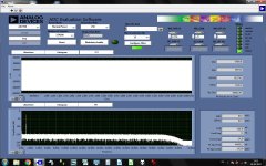
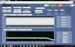
... Ok, so this is really weird ... I was about to set up things to do the 7 kHz cut-off frequency measurement and to this end removed the local FF decoupling capacitor I was using (220nF, 1210 size, C0G). I forgot to put it back in place and connected the PSU and did the THD measurements. The FF (74AUC1G74) now was decoupled only with a 470uF, 16mm diameter, 7.5mm lead spacing capacitor ... 😳
And the attachments are what I measured (same setup as earlier). To my surprise the distortion has actually dropped for DSD128 - now at ~ -108 dB - but very surprisingly now DSD256 is at ~ -102 dB! Please note that the No. of samples are not the same for both measurements as my computer isn't fast enough to play back DSD256 at any appreciable length. So a lower No of samples were taken for the DSD256 measurement. This at least also partly explains the higher noise floor with DSD256.
I am a bit at a loss of interpreting what is happening here - other than that xx3stksm may have a point about O&U. With this in mind my guess is that the inductance of the PCM 7.5mm capacitor is so high at higher frequencies that it actually dampens the FF - and thus reduces O&U significantly. And now the distortion rise between DSD128 and DSD256 is about 6 dB - which is more in line with my intuitive "assumption" of what it "should" be.
This is good enough for me
Thanks to all of you for commenting & helping out
Jesper
Attachments
It is not usually recommended to use C0G decoupling caps, nor recommended to use physically large ones such as 1210 SMD. Too little damping especially with too much parasitic inductance can lead to problematic ringing. Maybe less of a problem with slower devices since the slower switching transients on the power pins may provide less excitation for ringing.
EDIT: Too much capacitance can cause problems too. Sometimes faster devices need smaller capacitance values to keep self resonance above the switching excitation frequency.
EDIT: Too much capacitance can cause problems too. Sometimes faster devices need smaller capacitance values to keep self resonance above the switching excitation frequency.
Last edited:
Wild guess: the current that the flip-flop draws will be data dependent and will probably not have a white spectrum. Maybe the decoupling resonates at an unfortunate frequency.
From 0 Hz to half the sample rate, the spectrum of a DSD signal with a test tone consists of a region with very low noise and a test tone, a region where the quantization noise increases and flattens out, and a region that looks like an FM spectrum due to the modulated idle tone. Between half the sample rate and 1 time the sample rate, you get the same in the opposite direction. Above 1 time the sample rate, the whole pattern repeats.
I don't know what the spectrum of the supply current of the flip-flop looks like, but as it depends on the DSD data, it could very well be that it is not white. Maybe the two parallelled capacitors with their PCB traces have a parallel resonance at a frequency where the flip-flop draws a lot of signal-dependent current in DSD256 or DSD512 mode, but not in DSD64 or DSD128.
If any of this is true, then an RC network in parallel with the decoupling might solve it, but the trick is to find out how to dimension it - or just use one capacitor.
Regarding my RTZ shift register DAC: it is designed to draw an as nearly as possible data-independent current from the reference. That is, the current drawn from the reference will consist of bit clock harmonics and almost nothing else. When the reference gets polluted by exact multiples of the bit clock frequency, nothing bad happens; it only mixes down those parts of the spectrum of the DSD signal that are copies of the desired spectrum. Therefore, the reference decoupling should be less critical than with data-dependent reference current.
If ringing on power lines of the PCB is a problem, a one ohm resistor in series with a 0.1uF capacitor should help. Put one of these across the power pins of each chip for good measure. The book "High Speed Digital Design" goes into calculating "exact values" for such an RC circuit for a particular PCB, but just using these as standard values should help a lot if that's the problem.
In the case of an analog FIR filter composed of multiple taps, the AK4499eq has an advantage concerning switching. This is due to the small differences in tap characteristics and the negligible wiring lengths. However, it's worth noting that with the AK4499eq, I/V conversion is mandatory, and the selection of the operational amplifier to use is quite challenging. While D90 manages the issue well, DIY DACs often exhibit significant distortion. I suspect that there might be a specific op-amp for which the characteristics are finely tuned, allowing for corrections. There could be undisclosed registers or features that are not open for a DIYer.😕So it's better AK4499eq than FPGA?
I always suspected upsampling to higher rates poluted more the power rails.
Due to such challenges, overall performance-wise, even a discrete design with FPGA (DSD128) could achieve characteristics comparable to the AK4499eq, considering these factors.
Another Good morning to you all 😊
@MarcelvdG : Thanks once more for considering & commenting, Marcel. Sounds feasible what you are suggesting with data dependent noise, current draw and an RC network. Also in line with what @benb suggests, I reckon. One question here: Would a spectrum analyzer (up to 900 MHz) be able to show such VDD noise - and given "but the trick is to find out how to dimension it" - are there any noise spectrum clues to look for? I mean "probably" reasonably clean spectra around the actual sampling frequencies - but would there be something else/better to look for? A "trick" to handle the dimensioning trick
Sounds like good thinking ... !
@benb: Hi, & thank you also for your feedback 😉 As it is I actually have the book you mention - would you happen to remember just approximately (which section) where in the book this calculation can be found?
@Markw4 : Thank you also for chiming in ... I am aware of aspects of this - just didn't think it would matter that much in this context.
@xx3stksm : Hmmm ... slightly off-topic but nevertheless: I would like to compliment you for most always illustrating your points with measurements or illustrations of some kind. Very often I have found those to be very helpful & educative - and I also often find myself remembering some of these illustrations/measurements while considering "something". So many thanks for doing this! And then ... on a slightly different note: I am somewhat envious of your oscilloscope Must be great to be able to measure up to 5 GHz (or more) with all of the information and precision this entails - although I reckon such an oscilloscope isn't exactly cheap ...
Wouldn't that be the OPA1612 or OPA1632? I remember having seen "something official" from AKM where one of these opamps were used ... ???
Best wishes for your day 😉
Jesper
@MarcelvdG : Thanks once more for considering & commenting, Marcel. Sounds feasible what you are suggesting with data dependent noise, current draw and an RC network. Also in line with what @benb suggests, I reckon. One question here: Would a spectrum analyzer (up to 900 MHz) be able to show such VDD noise - and given "but the trick is to find out how to dimension it" - are there any noise spectrum clues to look for? I mean "probably" reasonably clean spectra around the actual sampling frequencies - but would there be something else/better to look for? A "trick" to handle the dimensioning trick
it is designed to draw an as nearly as possible data-independent current from the reference.
Sounds like good thinking ... !
@benb: Hi, & thank you also for your feedback 😉 As it is I actually have the book you mention - would you happen to remember just approximately (which section) where in the book this calculation can be found?
@Markw4 : Thank you also for chiming in ... I am aware of aspects of this - just didn't think it would matter that much in this context.
@xx3stksm : Hmmm ... slightly off-topic but nevertheless: I would like to compliment you for most always illustrating your points with measurements or illustrations of some kind. Very often I have found those to be very helpful & educative - and I also often find myself remembering some of these illustrations/measurements while considering "something". So many thanks for doing this! And then ... on a slightly different note: I am somewhat envious of your oscilloscope
Must be great to be able to measure up to 5 GHz (or more) with all of the information and precision this entails - although I reckon such an oscilloscope isn't exactly cheap ...I suspect that there might be a specific op-amp for which the characteristics are finely tuned, allowing for corrections.
Wouldn't that be the OPA1612 or OPA1632? I remember having seen "something official" from AKM where one of these opamps were used ... ???
Best wishes for your day 😉
Jesper
Last edited:
I have zero experience with such measurements, but if I were to try it, I would do something like this:
You could couple your spectrum analyser to the flip-flop supply through an AC coupling capacitor and a 470 ohm series resistor (to keep the 50 ohm analyser input impedance from damping the resonance, if any), and see if you see any suspicious bumps in the spectrum while playing DSD256 or DSD512, bumps that aren't there when you stop the clock and data. If you see any such thing, check what happens when you switch back to DSD128.
You could couple your spectrum analyser to the flip-flop supply through an AC coupling capacitor and a 470 ohm series resistor (to keep the 50 ohm analyser input impedance from damping the resonance, if any), and see if you see any suspicious bumps in the spectrum while playing DSD256 or DSD512, bumps that aren't there when you stop the clock and data. If you see any such thing, check what happens when you switch back to DSD128.
- Home
- Source & Line
- Digital Line Level
- The Best DAC is no DAC