Two corrections: some leftover components removed and ferrite bead-C filter added for the +5Vraw domain to reduce crosstalk from +5Vraw to other domains.
Is this circuit before the op amps basically converting/cleaning the DSD signal into what you'd find on the output of the old CS4303?
Anyone built this and know how effective it is (no audible noise/distortion)?
I've been interested in building a digital power DAC for headphones based on IVX's design, but taking advantage of PC based conversion and also making it compatiable with upcoming FIFO from Andrea.
The best and probably the only way to do it is by sending DoP to the FIFO, have the FIFO board drive an Ak4137 which just unpacks the DoP data and then have a converter like this before the buffer gate "output stage".
Im still unsure of the mechanism of noise/distortion a lot of us experienced with the raw noDACs but since reclocking with a flip flop is not enough to isolate the problem it seemed that it's related to the output of the digital logic when used in an analogue setting, rather than a problem with the input.
IVX managed to get exceptional measured performance with only simple buffer gate on the output which means one of 2 things, the problem is related to the input (it is a proper "analogue" pwm signal from TAS5558) or the large emount of gates in parallel achieves something similar to the above circuit
Last edited:
After reading back the best way to do this will probably be using flip flops in parallel rather than buffers since this seems to be giving the best measurements, and it could be clocked out directly by FIFO masterclock.
It would be differential flip flops for direct coupling,
increased distortion was noted with dual output flip flop by koldby so i will try seperate inverted and non-inverted flip flops in the hope that it helps, if differential outputs can minimise "white noise" issue that takes priority anyway.
Volume control is an issue... digital volume is possible but kind of sketchy with the logic outputing 7.6V peak all the time, and it would need nearly 10X attenuation for normal listening levels when SNR is already our biggest enemy with nodac.
Not sure if it makes sense but I thought about just having a low resistance voltage divider on each output to have an attenuator with reasonably low output impedance.
e.g 150R + 15R to ground would leave about 760mV with an acceptable <30R combined output impedance for 300 ohm headphones.
Load remains about the same for flip flops but resistive instead of inductive, might benefit from this...
Last edited:
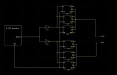
Is this circuit before the op amps basically converting/cleaning the DSD signal into what you'd find on the output of the old CS4303?
More or less; according to CRYSD001-2-3.pdf the CS4303 uses return-to-zero coding, but has no FIRDAC structure. The circuit of post #2237 ( https://www.diyaudio.com/forums/digital-line-level/273474-dac-dac-224.html#post5830769 ) combines return to zero with a short FIRDAC.
Anyone built this and know how effective it is (no audible noise/distortion)?
As far as I know, no-one built the exact circuit of post #2237 and in any case, the filter values and the muting circuit would require updating. It was derived from something quite similar that I did build, though, and that has 97 dB(A) dynamic range (about the noise floor of a CD player). See 74AHC02 and 74AHC08 DAC with 97 dB(A) dynamic range for details.
I've been interested in building a digital power DAC for headphones based on IVX's design, but taking advantage of PC based conversion and also making it compatiable with upcoming FIFO from Andrea.
The best and probably the only way to do it is by sending DoP to the FIFO, have the FIFO board drive an Ak4137 which just unpacks the DoP data and then have a converter like this before the buffer gate "output stage".
Im still unsure of the mechanism of noise/distortion a lot of us experienced with the raw noDACs but since reclocking with a flip flop is not enough to isolate the problem it seemed that it's related to the output of the digital logic when used in an analogue setting, rather than a problem with the input.
IVX managed to get exceptional measured performance with only simple buffer gate on the output which means one of 2 things, the problem is related to the input (it is a proper "analogue" pwm signal from TAS5558) or the large emount of gates in parallel achieves something similar to the above circuit
For a power DAC, it could be difficult to keep the reference/supply clean enough. Any disturbance on the reference except at exact multiples of the clock frequency can convert out-of-band quantization noise into the audio band or cause distortion.
By the way, almost all circuits in this thread are quite sensitive to second subharmonics on their clocks (harmonics are no problem, only subharmonics). I therefore wouldn't use them with clock generators involving frequency doublers, see https://www.diyaudio.com/forums/dig...itter-crystal-oscillator-285.html#post6373471 for some simulations illustrating the issue. The circuit of post #2237 of this noDAC thread should be somewhat less sensitive to this effect thanks to the four-tap uniformly-weighted FIRDAC structure. Basically each bit is converted four times and when the odd clock cycles are a bit longer than the even ones, the sum of the four bit weights ideally stays the same.
I wondered how IVX managed to get such got such good results with USB power in his power DAC.
The TAS5888 has 3 different PWM schemes it can use, only "AD" is comparable to balanced DSD. Also it seems to imply it's only running at 384kHz which is a huge difference when higher DSD rates had increased noise in basic noDac application.
The clock is only 5MHz without any doublers and probably isnt possible to use it for DSD with the FIFO at all.
The FIFO will have to truncate the DoP data to 16bit at 176kHz, the actual DSD data should still be intact but would need some special decoder to handle 16bit DoP.
Just seeing if anyone has any thoughts on this.
Attached are rough sketches of the 2 possible ways im going to try to build this power noDAC.
Chances are it will have unusable performance but it will be fun and costs so little.
In both examples the signals are "balanced" before the flip flops by an inverter and then inverting flip flops are used, first this keeps the signal path slightly simpler after the signals have been reclocked since non-inverting flip flops have a non-inverting buffer on the output (i.e 2 more inverters).
Additionally the single output flip flops dont have CLR and PRE functions, so their internal circuits are a lot simpler.
Finally, you have 2 seperate but identical flip flops working with inverse data inputs so it's more like a true balanced circuit than the dual output flip flop or a pair of non-inverting and inverting flip flops.
The initial idea, shown in the first example, was just to parallel the flip flops to increase output capability but there is also the possibility of using a single pair of the flip flops buffered by parallel inverters for the output stage, shown in second example.
The flip flops can achieve the same output capability but with a slightly simpler signal path.
Using inverters for the output will just move the heavy lifting from flip flop's output buffers outside instead with its own decoupling, depends how much the output load will effect the rest of the flip flop's operation.
but there is another pretty big difference to both examples...
With the flip flops you have many reclockers in parallel aswell, not just buffers, this has to have some adverse affect on the circuit. I dont have a hope of figuring out what that effect would be, or whether it is good or bad, without building both to see.
Im curious if the behaviours of this example can even be predicted with theory.
Attachments

Last edited:
Theoretically, with tripled flip-flops, you reduce the jitter of the flip-flops by square root of three as it averages out to some extent. No idea how big or small that effect is.
I don't know which of the two circuits causes the smallest data-dependent disturbance on the supply and ground. Chances are that that one will work best. If I had to bet, I'd take the one with the tripled flip-flops, as it doesn't have to charge and discharge the wires to the buffers and the buffer input capacitances.
What are you going to connect to the outputs and how much capacitance does it have?
By the way, one of the outputs in the left picture is not connected.
I was hoping some sort of effect like that might exist with the parallel flip flops.
There will be a lot more in parallel per signal in practice to share the load, at least 8, especially for flip flops since they will presumably be more sensitive and now considering this averaging effect. They (LVC1G80) are a ~10c part so not much limiting the number.
It is intended to drive headphones, but with my 'solution' for volume control mention at end of post 2262 they would only see a resistor to ground close to their output.
Another potential for volume control is a combination of digital control and lowering the supply voltage, but the recommended output current for the LVC logic family drops dramatically below 3.3V so probably no good.
In fact, if the output capability follows this trend in the other direction it might be a better idea to run the logic at 5V for this application. The IL715 isolator would convienently be able to provide level translation for it.
I think JohnW mentioned another benefit to running at 5V somewhere in the thread.
The headphone power DAC is working, no audible noise or obvious distortions like koldby's measurements suggested. Sounds fine in this state but still needs the isolator, which will add level translation for a 5V supply, which will be an ultrabib (currently lt3045) so too early to make judgements.
Very interesting!
Did you use the triple FF for this?
Did you make a PCB for it or p-p wiring?
What isolator are you planning to use?
Did you use the triple FF for this?
Did you make a PCB for it or p-p wiring?
What isolator are you planning to use?
No, single LVC1G79s.
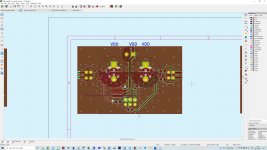
It is 4 layer PCB from JLC, cost around €5, it's crazy.
Isolator is IL715, I will add it today.
It is 4 layer PCB from JLC, cost around €5, it's crazy.
Isolator is IL715, I will add it today.
Just seeing if anyone has any thoughts on this.
Attached are rough sketches of the 2 possible ways im going to try to build this power noDAC.
Chances are it will have unusable performance but it will be fun and costs so little.
In both examples the signals are "balanced" before the flip flops by an inverter and then inverting flip flops are used, first this keeps the signal path slightly simpler after the signals have been reclocked since non-inverting flip flops have a non-inverting buffer on the output (i.e 2 more inverters).
Additionally the single output flip flops dont have CLR and PRE functions, so their internal circuits are a lot simpler.
hmm, how do you get balanced signal from paralleled circuits ? Anyway, thats true , a 6 // 74LS02 buffer from a 44,1kHz clock reduces jitter ...
Hi Koldby
what part You use for Your no-dac from page 214 this topic?
You just wrote
74LVC1G?
Is this 74LVC1G74
thanks 🙂
what part You use for Your no-dac from page 214 this topic?
You just wrote
74LVC1G?
Is this 74LVC1G74
thanks 🙂
No, single LVC1G79s.
It is 4 layer PCB from JLC, cost around €5, it's crazy.
Isolator is IL715, I will add it today.
How did it sound post isolator? Can more of these boards be produced if it sounds as expected?
Ups. Seems I missed the last 74 ;-). But it was a 74AUC1G74 as it is a FF...
thanks 🙂
How did it sound post isolator? Can more of these boards be produced if it sounds as expected?
Worse, the problem of jitter>isolation in this case.
In the end there was an underlying metallic-ness to the sound that could never be helped, probably related to poor high speed PCB design.
Also noticed some subtle artifacts in one channel , might have been a damaged/faulty flip-flop but couldnt be bothered building another or trying to find the fault so it was abandoned after that.
Managing volume was a problem, minimum supply of 1.65V (3.3V differential output) still requires heavy digital attenuation for my headphones and although there wasn't a huge difference I felt performance suffered going below 3.3V supply.
It might make more sense to scale it up for sensitive speakers instead of fighting the volume issue, you can get up to 11V differential output or 13V if you push to absolute max.
Last edited:
H
You said that single chip 4 X isolator IL715 used for digital isolation.
Maybe to use a single isolator for each digital line.
Like IL710.
(enable option could be of use too...)
.
I had good sonic results with ADuM1100 single isolators. 4 times for I2S bus.
Yes the jitter performance is probably slight worse, but in the other hand amount of digital noise is probably reduced?
.
Hi all,
I have been experimenting quite some with various versions of a NoDAC - basically a balanced FF with an RC filter on the output - and while I can get very reasonable results at DSD64 & DSD128 (-104 dB to - 107 dB THD at DSD128), when I try exactly the same circuitry at DSD256 or DSD512 the distortion goes up substantially (-79 dB THD at DSD256, and -67 dB THD at DSD512) - essentially no matter which FF I use.
Since this rise in distortion level is almost equal for all the FFs (74AC74, NC7SZ74, 74AUP1G74, 74AUC1G74) I have a feel that it may be something "structural" - either related to some for me unknown DSD conversion theory - or in the way I have designed the circuitry.
BTW - a slight digression: These simple NoDACs sound absolutely wonderful - the best I have heard in terms of resolution, tonality, spaciousness, and "naturalness" - so both out of curiosity and slight "bewilderment" I would really like to find out what may be happening here ..??
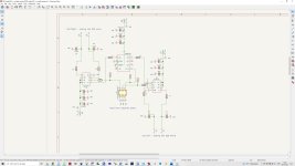
FYI I have attached a copy of the very simple schematic as well as the PCB layout. I use JLSounds' USB-to-I2S card with NZ2520SDA oscillators so the phase noise performance should be reasonably fine. The AD converter I use for measurements is the AD7760 which is a 24 bit 2.5 MHz Fs balanced input ADC (evaluation board) with a 1 kohm input impedance. Besides the RC filter on the output of the FF (4.7kohm and 5.6 nF to GND - loaded by the 1 kohm) I use no other filtering before entering the signal into the ADC.
If one of you may know what causes this rise in distortion I would much appreciate your feedback.
Cheers & thanks for considering 😉
Jesper
I have been experimenting quite some with various versions of a NoDAC - basically a balanced FF with an RC filter on the output - and while I can get very reasonable results at DSD64 & DSD128 (-104 dB to - 107 dB THD at DSD128), when I try exactly the same circuitry at DSD256 or DSD512 the distortion goes up substantially (-79 dB THD at DSD256, and -67 dB THD at DSD512) - essentially no matter which FF I use.
Since this rise in distortion level is almost equal for all the FFs (74AC74, NC7SZ74, 74AUP1G74, 74AUC1G74) I have a feel that it may be something "structural" - either related to some for me unknown DSD conversion theory - or in the way I have designed the circuitry.
BTW - a slight digression: These simple NoDACs sound absolutely wonderful - the best I have heard in terms of resolution, tonality, spaciousness, and "naturalness" - so both out of curiosity and slight "bewilderment" I would really like to find out what may be happening here ..??
FYI I have attached a copy of the very simple schematic as well as the PCB layout. I use JLSounds' USB-to-I2S card with NZ2520SDA oscillators so the phase noise performance should be reasonably fine. The AD converter I use for measurements is the AD7760 which is a 24 bit 2.5 MHz Fs balanced input ADC (evaluation board) with a 1 kohm input impedance. Besides the RC filter on the output of the FF (4.7kohm and 5.6 nF to GND - loaded by the 1 kohm) I use no other filtering before entering the signal into the ADC.
If one of you may know what causes this rise in distortion I would much appreciate your feedback.
Cheers & thanks for considering 😉
Jesper
Attachments

- Home
- Source & Line
- Digital Line Level
- The Best DAC is no DAC