struck by lightning
I find myself in complete agreement with Mr. Rollins. I plan to go build the thing and fine tune any issues like bandwidth or DC offset later. I may play with a servo later but find the 30 ohm resistor solution both reasonable and practicle, even for a commercial version. Analysis is paralysis. As Mark Twain said "Everyone talks about the weather but no one does anything about it." DC offset is diffcult to simulate be cause of thermal effects but very easy to measure, when a few of the Aleph Xs are bulit we can pool our experiences to address any concerns about offset. Back to the workbench.....
H.H.
My work in progress, please point out errors, and criticism is welcome.
Single sided, with just two jumpers and a bit of lead bending for Q5 & Q7.
R1, 2, 3, 4, 18, 19 28, 29, 42,43,44,45 are not on the board
Getting R19, 29 of the board helped alot, I would put them on the input connectors with R18, 28.
I used Proteuslite from <a href="http://www.labcenter.co.uk/">labcenter.co.uk</a> the bitmap is not to scale.
Regards
James
Attachments
It would be better if input differencial could share the same heat sink for temperature stability. You used jumpers to get connections for R9 and R38. Wouldn't it be better to put them on opposite sides and avoid jumpers?
Amazing how different things look after a good nights sleep, I will new post a PCB/Schematic after 4AM (Aust time) again.
The pads are a bit small, the 3w resistors aren't sized for 3W Metal Oxides, but the layout looks much better and is hopefully more accurate.
No jumpers and R18/28 are on the PCB.
Is mounting Q5/7 front to back a good idea, no one makes the same device with a mirrored pinouts that I know of.
Can post the Proteus layout file if anyone wants it?
Any comments??
James
Attachments
I don't see that differencial pair can use the same heatsink. It looks that the biggest complication in your layout are the traces from input differencial to the gates of output devices. You run them crossing ea. other. You have to run the trace between the legs of input mosfet and it means that the legs have to be bent quite a lot for different spacing. In my book it's no good. Mosfet should go into the board without need for leg "streching". Don't cross those traces, but run them in opposite directions. It doesn't change much because you connect wires to PCB anyway but the layout becomes better.
I just finished Aleph5 and put all 3 input mosfets on one heatsink. When I checked, it is pretty warm.
I just finished Aleph5 and put all 3 input mosfets on one heatsink. When I checked, it is pretty warm.
Hi Grey!
Just a short question what is the idle current in the current source for the diff pair?
What is the idlecurrent in the outputstage?
I am going to simulate this weekend (Maybe friday?).
I have trouble finding the model for the IRF9610. Do you have any ? Harry?
If i am not finding one i will try see if i can find another device close to the IRF9610 for the sim.... Not good!!
I have a small suggestion.. reduce the of the feedback resistor by 3 times (10k and 100k => 3k3 and 33k) and at the same time raise C2 and C4 3 - 5 times (33p - 47pF).
This should also have a influence (improve) on the phase margin ... But first i will do a sim with the original circuit.
When i have done this i will upload some curves on the freq. response.
Sonny
Sonny,
--The bias for the front end is about 20mA total, or about 10mA per side.
--Output stage bias is on the order of 2.27A for the circuit as published, i.e. with output bias set for .5V across the Source resistors.
--IRF models? None here. Sorry, I lost all my simulation stuff when the virus hit. I didn't even try to save that; the stories were more important. All I can do is suggest www.irf.com to see if they have it available for download. For accuracy's sake, keep in mind that I'm using IRF MOSFETs and OnSemi MPSA18s here, not Zetex '450s or any of the other likely candidates. Substitution may or may not give useful results...but on the other hand, someone is guaranteed to want to use the Zetex parts with Toshiba MOSFETs (or something...), so I'm sure that any simulation will be of interest to someone, somewhere. Just be sure to specify what models you use.
--Reducing the feedback will increase the measured distortion and reduce damping factor. Whether it will sound better or not I will leave to others. Bear in mind that the closed-loop gain will increase somewhat. This may or may not be a good thing, depending on your circumstances.
I'm still working on a PCB layout. (Have yet to look at the one posted above.) I've started a new pattern that may (if I'm lucky) allow me to post a single-sided board diagram. Maybe. It's slow going and further complicated by having a relative in poor health; my attention is divided at the moment. I'll keep plugging.
I still haven't built even one proper channel. Aside from the medical situation mentioned above, I need to commit to some sort of heatsink. Part of me says to go water-cooled (just build what I need), the other part says to go passive air cooled (in which case I'm at the mercy of what's available on the surplus market--you know that story).
As Pooh says,"Oh, <i>bother!</i>"
Grey
I just finished my layout it's a board with everything on it, it has a single layer and symmetrical (for the most part). However, I don't think it is quite mature for public scrutiny, yet. It will be awhile, quite frankly my motivation is terrible, it's the summer, it's hot and I am thinking more on the line of 'Corona with lime' rather than class A amps.
I am also trying to do a board with 3 mini-A on it which is going to be painful.
Grey,
sorry about your family problems. I hope everything is resolved for the best.
I am also trying to do a board with 3 mini-A on it which is going to be painful.
Grey,
sorry about your family problems. I hope everything is resolved for the best.
IRF9610 model
.SUBCKT IRF9610 10 20 40
* TERMINALS: D G S
M1 1 2 3 3 DMOS L=1U W=1U
RD 10 1 1.42
RS 30 3 76M
RG 20 2 83.3
CGS 2 3 155P
EGD 12 0 1 2 1
VFB 14 0 0
FFB 1 2 VFB 1
CGD 13 14 193P
R1 13 0 1
D1 12 13 DLIM
DDG 15 14 DCGD
R2 12 15 1
D2 15 0 DLIM
DSD 10 3 DSUB
LS 30 40 7.5N
.MODEL DMOS PMOS (LEVEL=3 VMAX=417K THETA=58.1M ETA=2M VTO=-3.1 KP=0.865)
.MODEL DCGD D (CJO=193P VJ=0.6 M=0.68)
.MODEL DSUB D (IS=7.47N N=1.5 RS=2.81 BV=200 CJO=151P VJ=0.8 M=0.42 TT=240N)
.MODEL DLIM D (IS=100U)
.ENDS
GRollins said:Sonny,
--The bias for the front end is about 20mA total, or about 10mA per side.
--Output stage bias is on the order of 2.27A for the circuit as published, i.e. with output bias set for .5V across the Source resistors.
--IRF models? None here. Sorry, I lost all my simulation stuff when the virus hit. I didn't even try to save that; the stories were more important. All I can do is suggest www.irf.com to see if they have it available for download. For accuracy's sake, keep in mind that I'm using IRF MOSFETs and OnSemi MPSA18s here, not Zetex '450s or any of the other likely candidates. Substitution may or may not give useful results...but on the other hand, someone is guaranteed to want to use the Zetex parts with Toshiba MOSFETs (or something...), so I'm sure that any simulation will be of interest to someone, somewhere. Just be sure to specify what models you use.
--Reducing the feedback will increase the measured distortion and reduce damping factor. Whether it will sound better or not I will leave to others. Bear in mind that the closed-loop gain will increase somewhat. This may or may not be a good thing, depending on your circumstances.
I'm still working on a PCB layout. (Have yet to look at the one posted above.) I've started a new pattern that may (if I'm lucky) allow me to post a single-sided board diagram. Maybe. It's slow going and further complicated by having a relative in poor health; my attention is divided at the moment. I'll keep plugging.
I still haven't built even one proper channel. Aside from the medical situation mentioned above, I need to commit to some sort of heatsink. Part of me says to go water-cooled (just build what I need), the other part says to go passive air cooled (in which case I'm at the mercy of what's available on the surplus market--you know that story).
As Pooh says,"Oh, <i>bother!</i>"
Grey
Sorry to hear about your relatives! They are more important than any hobby.
For the models. I think i have all the models i need know... The MPSA18 is from Fairchild though.
What i meant by the feedback network was not to lower the gain, but reducing the size of r18,r28 to 3k3 and r16,r26 to 33k. It will generate led distortion because of your Zenerdiodes capacitance and the mosfets input capacitance.... I know that you have a gate resistor but it will have an effect.. The dominant pole will also move up about 3 times.
The resistor noise will also be lower.
I will make sims for the original circuit and the circuit where i have reduced the values to 1/3.
Harry : Thanks!
Sonny
Grey,
How important is 10pF cap in a feedback loop? I didn't use it in my Aleph 5 (I couldn't find a good one) and it seems to be OK. I also didn't use 2 other small caps (1nF and 10nF) and no oscillations either.
😉
How important is 10pF cap in a feedback loop? I didn't use it in my Aleph 5 (I couldn't find a good one) and it seems to be OK. I also didn't use 2 other small caps (1nF and 10nF) and no oscillations either.
😉
The 10pF cap in the feedback loop sets the upper response of the amplifier to about 150kHz. Offhand, I don't remember what the upper limit is without the cap, but the circuit will try (more or less successfully) to do DC to light bandwidth without it. The top end at this point will be governed by the various MOSFET capacitances, the circuit layout, etc. The sum effect will be impossible to predict from where I sit; it'll be up to you to keep tabs on the stuff.
If you go without the cap, you'll be leaving yourself open to RF...and possibly circuit oscillation.
You'll also give Harry a heart attack.
My take is to proceed with caution. If your layout seems stable, and if your load isn't too reactive, and if you don't live too near a radio station, and so on...then you have my permission to experiment.
If in doubt, leave it in.
Note that Mouser and Digikey both sell silver-mica caps that will do just peachy. They're not very expensive, either. Mouser has nice little polystyrene caps in case you want to put the cap across the NPN. They're reasonably priced, also.
Another option is to alter the value somewhat. The smaller the cap, the higher your highs will go. To a first approximation, you can calculate the -3dB point simply by plugging in the 100k value of the feedback resistor. A 5pF cap, for instance, would give you a -3dB point in the region of 300kHz.
Again, proceed with caution, but you have my blessing to alter that value as long as you test thoroughly and take responsibility for your own smoke releases.
I ran both the Mini-A and the Aleph-X without the 10pF caps, and both circuits (at least here, and with the caveat that they were both built on these push boards, which raises the possibility of stray capacitance) were stable. At least in the Mini-A, adding the 10pF did damp a little overshoot on a 10kHz square wave. I can't remember what the square wave on the Aleph-X looked like, with vs. without. If I have time, I'll poke at the circuit tonight when I get home from work and report.
The caps across the NPNs, well...Harry feels they're necessary, Nelson indicates that they <i>may</i> be necessary, and I haven't needed them yet. Your Mileage May Vary.
Thanks for the well-wishes folks, the Grim Reaper has been seen in the neighborhood. Things will simply have to proceed as they will.
Grey
I've read over this thread and looked at the circuit, and have a couple of questions. Essentially this circuit seems to be a bridged Aleph with only one input section. Aside from eliminating a few input mosfets, what advantage does this circuit give you over simply bridging one stereo Aleph, and driving it with a balanced signal?
The main reason I ask this question is that with this circuit, the inputs are also where the feedback is sent. How much interaction might occur between the input and the feedback? With the bridged sterero Aleph, the feedback is somewhat isolated from the input signal as both the + and - input signals would be sent to non-inverting inputs and the feedback would be at the inverting inputs. (Would the DC offset be less of an issue in this case too?)
The other reason I ask this question arises from some listening tests that I've done with bridged amps. I've been playing with various bridged amps (discussed on the solid state forum), using STK4048XI and TDA7293V modules, as compared to a single-ended, non-bridged Aleph (home brew) and a Rowland model 10 amp (bridged using many LM3886 modules). During these comparisons, I also listened to amps with fully balanced inputs (+ and - are both sent to non-inverted inputs) versus those such as the basic Aleph that use a balanced input, but feed the - leg into the inverting input side (where the feedback is located).
The amps sounded much better when fully balanced (and bridged) as opposed to those where the - signal was presented to the inverting input. Therefore, I'm wondering if it's not better simply to bridge a standard Aleph and avoid feedback interactions. Comments?
Regards, Robert
feedback interactions
I would check Mr. Pass's article at:
http://www.passlabs.com/pdf/susy.pdf
There are also real avantages in running the inputs on each side as inverting stages in terms of reduction in commom mode signal seen by the input stage. In addition most Power supply noise components will appear as common mode components and will be rejected by a true balance differential amp. The topology also allows smaller supply voltages for a given voltage swing and therefor higher bias currents for a given idle power dissapation. Convinced yet?
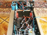
Attachments
HH,
I am convinced; thanks. I had not previously read Mr. Pass's article. It addresses just what I was wondering about.
BTW, very nice looking amp!
Regards, Robert
I am convinced; thanks. I had not previously read Mr. Pass's article. It addresses just what I was wondering about.
BTW, very nice looking amp!
Regards, Robert
Differential amplifier biasing
Harry,
the bias current for a class-A balanced output stage is not actually higher than that of a single-ended one - you just have two of them. The output transistors are not biased at a higher current relative to the signal current swing than they are in the single-ended case.
There is also a slight efficiency hit as you reduce the voltage rails because the biasing overhead (how close you can swing to the rail) does not decrease so becomes a larger fraction of the DC dissipation. However, anyone subscribing to this board will not be too concerned about that.
And the output resistance doubles compared to single-ended.
That said, I like balanced designs and I'll be interested to read how the Aleph-X compares to a single-ended Aleph. Will even-order cancellation in the Aleph-X enhance or detract from the Aleph sound?
Regards
13th Duke of Wymbourne
bias current for a class-A balanced output stage
The use of lower voltage rails allows one to bias the transistors higher for the same bias dissapation. Power equals voltage times current, less voltage is more current for a given power. The higher the bias current the greater the transconductance and lower the distortion for the amplifier. I plan to bias at about 2.5 amps which is about as far as I dare push the output devices with 16 volt rails.
H.H.
I agree with both HH and 13DoW but on different points.
The lower rails allow higher bias which is good but the bridged design also requires more output current anyway so you do not really gain extra bias current relative to output current.
The lower rails allow higher bias which is good but the bridged design also requires more output current anyway so you do not really gain extra bias current relative to output current.
bridged design also requires more output current anyway
What!!!!??? Assuming we are talking about the same votage swing into the same load impedance, I am afraid I don't follow your reasoning.
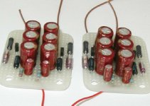
View of Zetex ZTX 450 boards for active current sources. Elna Cerafine elkos, Seimens polystyrenes, and Resista and Corning RN60D resistors.
What!!!!??? Assuming we are talking about the same votage swing into the same load impedance, I am afraid I don't follow your reasoning.
View of Zetex ZTX 450 boards for active current sources. Elna Cerafine elkos, Seimens polystyrenes, and Resista and Corning RN60D resistors.
Attachments
- Home
- Amplifiers
- Pass Labs
- The Aleph-X