Brian
series caps are high pass filters so the DC from your pre-amp doesn't wreck havoc in you nicely balanced, and symmetric, XA.
Ooops, just broke the 1000th reply, sorry!
series caps are high pass filters so the DC from your pre-amp doesn't wreck havoc in you nicely balanced, and symmetric, XA.
Ooops, just broke the 1000th reply, sorry!
Finally hit 1000 posts! 26 pages long of aleph-x...
Is it wise to include dc blocking input capacitors for the aleph x? 10uF film caps like the Zen V4? The aleph doesn't have them.
--
Brian
Is it wise to include dc blocking input capacitors for the aleph x? 10uF film caps like the Zen V4? The aleph doesn't have them.
--
Brian
They're entirely optional. I guess it depends on how much DC you think your preamp will contribute, as this will be amplified by the AX gain.
Brian,
Beautiful job!
I think the traces could be exactly symetrical if Q5 and Q7 were each turned 90 degrees but in opposite directions.
The + and - gate traces could then run off the end of the board on either side of the CCS trace. (or each turn 90 deg to the side)
The traces from R22 and R 27 would then run straight into Q5 and Q7
The trick is that the transistors face in opposite directions even though the holes for both can be in line. They could be bent horizontal and both attached to a heat sink above.
THEN you have asymetrical attachment to the heatsink?
Kinda. So you trade one asymetry for another, but at least the traces are identical! PRbably they won't attach right to any heatsink in the known universe 😉
Do I get the $100 ?🙄
BrianGT:
Going back to one of your older posts... double-sided is definitely the way to go for commercially produced boards. It results in easier layout, and the boards are a little more robust, since the plated through-holes tend to help prevent traces from peeling up at the pads.
Concerning symmetry, the exact trace length and precise mirror geometry aren't really ultra-critical. Remember also that any magnetic flux or electric fields which are not present symmetrically on the board will not be fully rejected by the circuit. But, it is nice to see a board which is fully symmetrical.
Your board layout looks like it's coming along very nicely. You're using Protel right? If so, there's a nice feature it has for "pouring" polygon planes to fill any space not consumed by traces and pads. You can define the clearance between the plane and other board features. This is what I use, and it's very handy, producing perfect results. Manual addition of polygons can be used to patch up areas that don't look right.
Lastly, with regard to the "unified" PCB effort, thank you very much for your offer to help. So far, you and carpenter are the only others who seem interested in contributing their time to do the layout work, so perhaps you and I can work together on the layout implementation in Protel 98?
Yep, you trade one symmetry for the other... unless you make creative use of a two-sided board, in which case, you can consider the traces on top and bottom sides to be nearly co-planar, due to the small thickness of the board. Following me? Now, you can make identical copper areas on each half of the board, and just have them connect to the pins at different points... Now your transistors can all face the same way for mounting on to a flat-faced heatsink (not possible with transistors facing opposite directions). There will of course be slight non-symmetries, but it's much closer than if you're restricted to a single layer.
Chad,
Thanks for the advice on the polygon plane. I have just been manually adding normal planes into the design as desired.
Is a crosshatched ground plane better? I assumed that more surface area is better for a ground plane.
I am using Protel DXP. I was using 98, but I only have the demo and it expired. I have a while left for DXP, then I can install the newest service pack for it and they give you another month. I am still pretty new with Protel, doing everything manually. I autoplaced and autorouted a graphic eq design for a friend and it came out alright. I enjoy the challenge of placing and routing the board manually, and after a few tries, I manage to get placement that I like.
I can send you the layout if you desire. Let me spend a bit more time on it get it to a state that I like, then I can send it out. I can see if I can export it in 98 format. I am planning on making the layout with Grey's schematic with a couple of changes, then after doing this, I can lay it out with Fred's modified CCS. I can't decide it I should just prototype the circuit on my protoboard first, or get two seperate pcbs made.
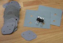
Question: I can get double sided boards made for me at school here, which are done with a milling machine, then plated. They don't have a solder mask, so I am wondering what the best way to insulate the heatsinks from the board, so that I don't ground out stuff. I was thinking about just finding some plastic film to sandwich between, or coating it with something like polyurethane. Any suggestions on a good way to go about this? McMaster sells teflon sheets, with I considered I just cut up some mica to-3 insulators for my leach amp board for under the two heatsinks:
http://brian.darg.net/leachamppcb/abp
On a side note, microchip.com started a samples program for their PIC microcontrollers.
--
Brian
Thanks for the advice on the polygon plane. I have just been manually adding normal planes into the design as desired.
Is a crosshatched ground plane better? I assumed that more surface area is better for a ground plane.
I am using Protel DXP. I was using 98, but I only have the demo and it expired. I have a while left for DXP, then I can install the newest service pack for it and they give you another month. I am still pretty new with Protel, doing everything manually. I autoplaced and autorouted a graphic eq design for a friend and it came out alright. I enjoy the challenge of placing and routing the board manually, and after a few tries, I manage to get placement that I like.
I can send you the layout if you desire. Let me spend a bit more time on it get it to a state that I like, then I can send it out. I can see if I can export it in 98 format. I am planning on making the layout with Grey's schematic with a couple of changes, then after doing this, I can lay it out with Fred's modified CCS. I can't decide it I should just prototype the circuit on my protoboard first, or get two seperate pcbs made.
Question: I can get double sided boards made for me at school here, which are done with a milling machine, then plated. They don't have a solder mask, so I am wondering what the best way to insulate the heatsinks from the board, so that I don't ground out stuff. I was thinking about just finding some plastic film to sandwich between, or coating it with something like polyurethane. Any suggestions on a good way to go about this? McMaster sells teflon sheets, with I considered I just cut up some mica to-3 insulators for my leach amp board for under the two heatsinks:
http://brian.darg.net/leachamppcb/abp
On a side note, microchip.com started a samples program for their PIC microcontrollers.
--
Brian
Insulating boards...
I use scotch tape for this at work. 😀
Electrical tape works too. Just don't try soldering near it, or it melts and makes a stink and a mess... If you need heat resistance, then Kapton tape (polyimide tape, Kapton is the 3M name) is good.
I use the crosshatch type, but make the width/spacing ratio greater than one so that it becomes solid. You can strengthen a board with little squares.. basically a reverse crosshatch of isolated copper squares. Do feel free to forward the files to me. I'll tell you if they work correctly in '98.
sound of aleph x?
Hi,
are there any sound comparisons of aleph x or descriptions in this thread?
If not, how is the sound in comparison to SOZ? - if someone has experiences here...
thanks,
Ralf
Hi,
are there any sound comparisons of aleph x or descriptions in this thread?
If not, how is the sound in comparison to SOZ? - if someone has experiences here...
thanks,
Ralf
AX has symetric input. Most of players are euiped by asymetric output. Do you use any symetrising circuit for AX?
Koy
plan to use BOSOZ, straight up no CCS. Best sounding preamp I ever built.
I expect the pair will sing like a hummingbird.
Pass creations are extraordinary.
plan to use BOSOZ, straight up no CCS. Best sounding preamp I ever built.
I expect the pair will sing like a hummingbird.
Pass creations are extraordinary.
Brian
if you have a linux machine in the lab you could use
http://bach.ece.jhu.edu/~haceaton/pcb/
I have heard good things about it.
if you have a linux machine in the lab you could use
http://bach.ece.jhu.edu/~haceaton/pcb/
I have heard good things about it.
sound of aleph x?
Didn't someone post a comparison with the Zen a few pages back? Carpenter, I think...
Didn't someone post a comparison with the Zen a few pages back? Carpenter, I think...
...and that's my own PCB
This is my own PCB for Aleph-X 🙂
That's my first Aleph design and also my first double-sided pcb design, I hope there are no mistakes in it.
To have traces and layout simmetrical, I will mount the Mosfets vertical on the PCB, they will be coupled with a screw to an alluminium angular attached to the heatsink.
Tell me what you think about.
This is the first side🙄
Bye, Fabrizio
Attachments
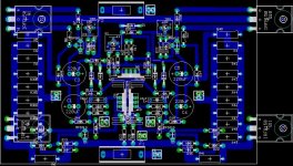
Looks pretty good. I think you can safely get rid of the fuses there is no point in having them in SE class A. You would be putting a 10-15 Amp fuse that would blow when the house is on fire, maybe. Could use the extra room for the input caps.
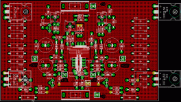
Hi to everybody.This is my proposal for an AlephX layout.It is close as the one I will realise by hand.Note that the unit square on my drawing is 5 mm and not 5.08 . This is because I have only normal paper.However,the final layout will be 5.08 space standard.
I have a few jumpers.I don't consider it badly,I just get rid of longer connections that way.The board is single sided,and the total layout is quite small anyway.It is also easyier to replicate than double-sided boards.
I intend to go with a total of 8 power devices.This choice is dictated by the fact I have hundred of IRFP240 in stock.Each device is intended to run at slightly more than 1 Amp bias on +/-22V power supply.I think it is right about safety power dissipation margin.Oh,I have included the Magical resistors from output nodes to sources of the differential.And I tried to go for most symmetric possible layout.
Any feedback welcome,as it is not realized yet.I am in no hurry.all thanks goes of course to tvi ,for inspiration.
Best regards to you all
Anael
PS.Warning.The board is not tested.But I guess I have no mistakes in it 😉😎
Attachments
These layouts are extremely good, particularly Fabrizio's
(Love that name).
But I want to point out something, which is that while
they are symmetric geometrically, they will still tend to
pick up stray magnetic field. Not much, but some.
Of course you can keep them away from transformers, which
I recommend anyway.
For the ultimate, though, we want to take this symmetric
layout and fold it at the middle, so that each half experiences
the same magnetic field.
For the XA200 and XA160 so far, I have intermingled the
placement of each half to achieve much the same thing -
we want the symmetric halves to experience exactly the
same magnetic field.
😎
- Home
- Amplifiers
- Pass Labs
- The Aleph-X