Persist with "unified" PCB effort?
I see several members have made excellent progress in making their own board layouts. Shall I continue to drive an effort to develop a "unified" PCB for general use and mass purchasing? If there is still support for this, I would like to start by calling for all interested persons to reply and/or email me with a short message. I will compile a list of participating members and start coordinating the effort from there.
If you're interested, please indicate one of three categories:
1. people who just want to get in on the group buy at the end
2. people from 1. who also want to have input on the board design and layout
3. people who are willing to contribute their designs as a starting point, and/or can help with the layout... (tvi, BrianGT, grataku?)
Pass DIY Addict
Joined 2000
Paid Member
I too, am a member of Group #1. I'd like to purchase a set of boards after they have been sufficiently critiqued and refined.
Eric
Eric
I would like to try to help out and be part of group #3. I really would like to see this design mature. I realize that there are better pcb designs out there then the one that I am working on, but my current plan is just to do my own layout and have my own boards made, as I see this more of a learning experience then anything else. I don't really get much from this if I take someone else's board and slap the components from a list on it and call it done.
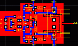
Should the board design stay single sided? For a group pcb order, double sided seems the way to go, since they are going to a production house anyway and double sided boards don't really cost any more $. Double sided boards give more design options: shorter traces, ground and vcc planes, and more. Looking over grataku's layout, you can see the increased symmetry that double sided pcbs can offer.
On the other hand, if it stays single sided, almost anyone who knows how to etch a board can download the pics, make the films and etch their own pcbs. This also allows prototypes can be easily made and tested before organizing a group order.
As for the circuit, has anyone tested both the original grey's ccs vs the revised fred ccs?
As far as symmetry goes, if the traces are the same length, but don't run the same path (due to the assymetrical nature of mosfets), is this alright?
--
Brian
As for the circuit, has anyone tested both the original grey's ccs vs the revised fre
You're a double EE student! Make like a busy bee and go test it yourself you slacker. I'll bet Professer Leach will even give you extra credit. The difference in PSRR for the voltage reference is several orders of magnitude by the way.
Youth is wasted on the young,
Fred
You're a double EE student! Make like a busy bee and go test it yourself you slacker. I'll bet Professer Leach will even give you extra credit. The difference in PSRR for the voltage reference is several orders of magnitude by the way.
Youth is wasted on the young,
Fred
I will test it myself eventually, but I don't have the parts for it now. I am gathering parts for the original posted circuit now, so I guess I will look for those parts too.
--
Brian
--
Brian
BrianGT said:
Should the board design stay single sided? Double sided boards give more design options: shorter traces, ground and vcc planes, and more. Looking over grataku's layout, you can see the increased symmetry that double sided pcbs can offer.
On the other hand, if it stays single sided, almost anyone who knows how to etch a board can download the pics, make the films and etch their own pcbs. This also allows prototypes can be easily made and tested before organizing a group order.
As far as symmetry goes, if the traces are the same length, but don't run the same path (due to the assymetrical nature of mosfets), is this alright?
--
Brian
It doesn't really matter for home made boards process, if they double or single sided. It just double the work and the difficulties level is not increased for that matter. However, if double sided layout simplifies the traces, by all means go for it.
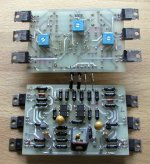
Check my A75 boards. Although I did them 8 years ago, by hand, I still consider them a thing of beauty. The six FETs mount directly to the chassis, so heat sinks are not required. This boards had to be double sided.
As to your question about symetry, don't get to concerned with it. Because of leads config on devices you will never be able to achieve perfect layout. Just try to achieve similar traces lengths and shape.😉
Attachments
I think single side boards are a thing of the past, if enough people are willing to do it pcb boards can be purchased for peanuts, literally.
There is no way someone etching his or her own board in the basement could be achieving the result of a commercial pcb manifacturer, not to mention the environmental clean up. I remember dumping Fe2Cl2, Fe3Cl3 and Cu2Cl2 cocktails down the drain and cleaning the flux with freon, I was 12, didn't know any better. Also remember that single face pcb without metallized holes are pretty much a one shot deal. Removal of a component more than once and the trace will peel right off.
In a non-profit situation, the cost of prototyping could be included in the final price of the production boards and still come up to a board that cost 5 times less than some of the Pass clones I saw on this and other sites around. More to the point I am rapidly converging to a final design although I'll maybe sacrifice a little symmetry for ease of mounting the output transistors, I haven't decided, yet, I am getting ready to send the file out to print.
This will be a prototype, no mask or component layout. It's going to cost me about $100 bucks to make a pair and that is what I am going to do if no one is interested. Of course I would like to share the $60 setup charge amongst a few "friends".
One thing my Pcb won't be called is "clone". I like to think I have the original.
Fred,
There has been a lot of (well, a little) talk about running the CCS ground to V- for added performance. Would the be appplicable with your design as well, assuming the Current Ref FET (J505) could handle the V+ to V- voltage?
There has been a lot of (well, a little) talk about running the CCS ground to V- for added performance. Would the be appplicable with your design as well, assuming the Current Ref FET (J505) could handle the V+ to V- voltage?
Wessol,
should have looked at this before emailing you. My layout allows you to do that or to go to ground or to use Grey CCS. I plan to go to -15V, so it better be possible! I think the value of the resistor may need to be doubled, that should be all. Something to test out.
should have looked at this before emailing you. My layout allows you to do that or to go to ground or to use Grey CCS. I plan to go to -15V, so it better be possible! I think the value of the resistor may need to be doubled, that should be all. Something to test out.
Would the be appplicable with your design as well
Probably not.... the point of the negative supply connection was to make the resistor bigger for the same zener current. Try a 1 mA current diode if designing from scratch, higher impedance than J505.
READ THE DATA SHEETS,
Fred
Probably not.... the point of the negative supply connection was to make the resistor bigger for the same zener current. Try a 1 mA current diode if designing from scratch, higher impedance than J505.
READ THE DATA SHEETS,
Fred
Re: Would the be appplicable with your design as well
Isn't the J505 a 1mA current diode? Does anyone know a good place to get these? Mouser carries them, but hasn't had any in stock for a while.
http://www.mouser.com/index.cfm?handler=listproduct&&categoryid=93&lst_pcode=7819
Data Sheet:
http://www.vishay.com/document/70196/70196.pdf
Any suggestions on a supplier? I searched and couldn't find any other suppliers.
--
Brian
Fred Dieckmann said:Probably not.... the point of the negative supply connection was to make the resistor bigger for the same zener current. Try a 1 mA current diode if designing from scratch, higher impedance than J505.
Isn't the J505 a 1mA current diode? Does anyone know a good place to get these? Mouser carries them, but hasn't had any in stock for a while.
http://www.mouser.com/index.cfm?handler=listproduct&&categoryid=93&lst_pcode=7819
Data Sheet:
http://www.vishay.com/document/70196/70196.pdf
Any suggestions on a supplier? I searched and couldn't find any other suppliers.
--
Brian
HiFiZen lucid explanation was:
"The advantage of running R17 to negative rail instead of ground is two-fold. First, it will be a larger value resistor (almost twice). This is good for rejecting ripple and noise, since the current flowing through it will be generated by a larger voltage across a higher resistance (remember, an ideal current source has infinite impedance). Second, it avoids having supply currents to ground. This prevents DC imbalance between the positive and negative rails, however small it may be. That last point is just a minor nitpick here, but in other circuits it would likely matter more... Nevertheless, the first point remains valid: the CCS will have better performance with this one very simple change, and you shouldn't have to modify and cap values to do it, just the resistor value."
J5xx doesn't really mean anything, current vary across brands.
Siliconix J505 is 1mA.
http://www.vishay.com/brands/siliconix/SSFsgcrd.html
According to my calculations for the 1mA to -15V R17h=~19Kohms is needed, for 4.7mA R17~4k Siliconix j505 and J511, repectively.
So the whole thing should be work just fine as I said.
Can the resident EE confirm these numbers? ?
?  ?
?
Goodnight.
"The advantage of running R17 to negative rail instead of ground is two-fold. First, it will be a larger value resistor (almost twice). This is good for rejecting ripple and noise, since the current flowing through it will be generated by a larger voltage across a higher resistance (remember, an ideal current source has infinite impedance). Second, it avoids having supply currents to ground. This prevents DC imbalance between the positive and negative rails, however small it may be. That last point is just a minor nitpick here, but in other circuits it would likely matter more... Nevertheless, the first point remains valid: the CCS will have better performance with this one very simple change, and you shouldn't have to modify and cap values to do it, just the resistor value."
J5xx doesn't really mean anything, current vary across brands.
Siliconix J505 is 1mA.
http://www.vishay.com/brands/siliconix/SSFsgcrd.html
According to my calculations for the 1mA to -15V R17h=~19Kohms is needed, for 4.7mA R17~4k Siliconix j505 and J511, repectively.
So the whole thing should be work just fine as I said.
Can the resident EE confirm these numbers?
? ?Goodnight.

I will start trying harder then 🙂
Is this the right way to do the ground plane? I was copying it off of the pass labs pictures. Other ground planes that I have seen seem to have the ground too close to the signal traces.
--
Brian
Is this the right way to do the ground plane? I was copying it off of the pass labs pictures. Other ground planes that I have seen seem to have the ground too close to the signal traces.
--
Brian
Please note that original XA board contains only 2 zeners (instead of 4) as Gate-Source protection. As to grounds, I don't have much experience here.
I posted a page ago about the two zeners and Mr. Pass said the ones in the XA are for gate-source protection.
There are also big input capacitors on the XA front end. What is the advantage of having these?
--
Brian
There are also big input capacitors on the XA front end. What is the advantage of having these?
--
Brian
- Home
- Amplifiers
- Pass Labs
- The Aleph-X