Member
Joined 2009
Paid Member
I used the KiCAD files posted in #1131 by @longface54 - he imported them into KiCAD and updated the BOM information.

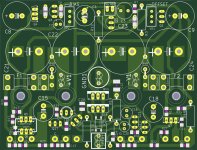
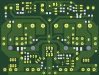
I don't see a designation on the large TO-247 Fets and BJTs, would help so they don't get put in wrong spot. Also looks like you named the first leg on all 4 large outputs as "G", (2) should be "G" the FETs, and (2) should be labelled as "B" the BJTs. Changing one or both of these would assist with confusion on placement location.Attached the updated PCB: protection circuit as shown in #1169, and as the board is rather crouded I tidied up the silk print so that the reference of each part is visible. What else can be done?
Great job - appreciate all the work, I have two original boards, I'm still holding onto for future use.
EDIT - nevermind - I see you put them on the back silkscreen. Thanks.
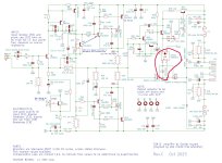
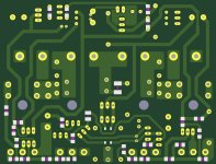
Attached the corrected silk print, I also rounded the corners of the copper areas, and the only small mod to the schematic is marked in red (because the opto coupler is not in stock at mouser):
Attachments

Member
Joined 2009
Paid Member
My intent with the GND traces was to create a kind of ‘star ground’ ref point with the ‘last caps’ on the power rails. If this point can be ‘cleaner’ with the proposed edit then why not, we’ll take every bit extra performance ! Of course, you also want to have these caps electrically ‘right close‘ to the power devices as they are the lowest impedance path for the audio return currents from the speaker.
Last edited:
There are extra caps near the output devices, so I think enough close / low impedance path. But maybe we can improve on that if we delete the R from the CRC before the power section and filter the front end with it's own CRC?
Member
Joined 2009
Paid Member
Could be interesting. Remember, the impedance of a cap depends on it’s capacitance, large caps being lower impedance.
I did not experiment much with this amp, it just came out of the gate with a sound I couldn’t fault which left me with no direction to go in afterwards. So I decided for the TGM8, that I didn’t want to mess with it (a higher power version has been mulled over but I prefer high efficiency speakers so the need has yet to appear, and a Class A version has been mulled over but I’ve found valves suit me nicely in that Class).
Your build is your journey, and you should ‘put your stamp on it’. You could try and leave flexibility in the design of the pcb, resistors can be replaced by links for example and you can put off-board power supply parts into the chassis. I used a cheap bridge rectifier, pretty sure you can do better.
Last edited:
Member
Joined 2009
Paid Member
I remember now that I used ‘snap-in’ power rail caps. The holes on the pcb weren’t sized properly for that as I didn’t interpret the datasheet drawings properly and the holes were slightly over-sized. The caps were not ‘snapping in’ as I would have expected (it’s the only time I’ve used snap-in caps) and I do like their solid meaty terminals. You can check to see if the last version I posted still had that issue and fix it on your design if using the same caps.
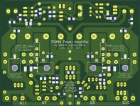
OK, here are my Kicad files: I did a lot of small retouching such as moving SMDs which were sitting too close to each other, or improving thermal separation between pads and copper areas (all for better soldering), so no big changes, just a lot of small stuff that should make assembly easier. The snap-in hole size was fine BTW. GND layout in the input section is improved as well. Other than that I tried to keep as close as possible to the original spirit of the layout. @Bigun, you mentioned that you want to move from Eagle to Kicad iirc, so I hope you can use my work as a starting point for your future plans with the TGM8 (if there are any).
Attachments
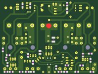
Actually the power-GND layout is still not good, I will rework it again. The wire coming from the rectifier should connect between the main caps (marked red in attached picture), and from there T'd away the cleaner GNDs should be connected. Otherwise these other connections "see" the dirt on the 0V line between caps and rectifier. I guess the solution is to isolate the connector from the star point...
Attachments
Member
Joined 2009
Paid Member
Member
Joined 2009
Paid Member
Looking at your posted images I don’t see traces narrower than the pads which is fine. I prefer fat traces, even if the thinner traces are good in terms of current handling I feel that fat traces are more robust and less likely to get damaged or lift with a hot iron. I haven’t started using KiCad yet, maybe it has some built in tools or design rule check where you can set a minimum trace width and it’ll warn you if there’s a concern. In terms of current, it is often possible to order pcb’s with thicker copper for an extra fee.
Depending on your skill and experience, you might like to use larger - elongated pads for the SMD opto device so that it’s easier to install by hand.
Depending on your skill and experience, you might like to use larger - elongated pads for the SMD opto device so that it’s easier to install by hand.
Thanks for the hints! OK, I will use an improved footprint for the opto. Kicad has a nice check tool, and I will use 2oz PCBs, so I hope it will be fine like that.
Kicad is easy to work with once you get used to it. Only at the beginning it can be confusing how everything is linked together in that software package - but now I appreciate it a lot, even editing the schematic or PCB files with a text editor and use search/replace to batch replace parts etc. is possible...
Kicad is easy to work with once you get used to it. Only at the beginning it can be confusing how everything is linked together in that software package - but now I appreciate it a lot, even editing the schematic or PCB files with a text editor and use search/replace to batch replace parts etc. is possible...
Member
Joined 2009
Paid Member
I read that KiCad has a built-in Spice circuit simulation tool. Have you tried using it? If so, how well does it work in your judgment ?
- Home
- Amplifiers
- Solid State
- TGM8 - my best amplifier, incredible bass, clear highs, no fatigue (inspired by Rod Elliot P3a)