Member
Joined 2009
Paid Member
Connect + and - together, and then to the chasis. Connect one (or both) of the S to the amplifier ground.
Ok brilliant - I'll get it wired up, put the lightbulb in series and fire it up.
Let's see if we can bring the world's third TGM8 to life (unless there are other siblings we don't know about out there....).
Let's see if we can bring the world's third TGM8 to life (unless there are other siblings we don't know about out there....).
Member
Joined 2009
Paid Member
Sounds good!
(hope you put insulator pads or mica washers between power devices and heatsink!)
yes, you bet, i've put some insulator pads and some thermal grease, cheers Gareth.
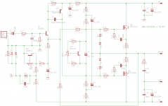
...........I'm just finishing up the wiring of my TGM8 (original version) and have used the attached diagram (courtesy of DIYAUDIO member richie00boy) as a layout reference.
Is anyone able to advise what value (voltage + uF) capacitors in the diagram would be suitable for 35vdc post-rectified supply? Also - what is the actual purpose of these capacitors?
This is wrong. DO NOT take the Speaker Return to the PSU Zero Volts link. See later.These capacitors filter the charge pulses coming off the rectifier, acting as integrators to provide a smoother d.c. voltage to the amplifier. They also provide a return path for signal current returning from the speaker ground connection back to the bridge rectifier. ...................
The two capacitors are the PSU smoothing capacitors. They pass the charging current pulses from the transformer via the rectifier. This MUST be assembled as a Group with a VERY LOW LOOP AREA. All the Flow and Return Pairs must be twisted, or at very least close coupled as Flow and Return Pairs..........................I don't have a variac, but can certainly wire the amp in series with a light bulb.
Re the ground, I drilled the ground hole about 15cm away from the IEC socket on the base panel on the chassis, and have it connected via a lug to the IEC socket, the centre tap of the transformer, the speaker GND and the GND from the PCB.
So it would appear that the distance from the IEC socket to the star/chassis ground is OK, I just need to remove the 'other grounds' (speaker, pcb, centre tap) and solder a pair of diodes between the chassis ground and the 'other grounds'. As attached?
The first diagram shows the link between the caps (PSU Zero Volts) having lots of other connections. One connection goes to each capacitor, one connection goes to the Centre Tap, one connection goes to the Main Audio Ground (MAG).
DO NOT locate the MAG on the PSU Zero Volts Link.
Instead you MUST locate the MAG off the Zero Volts. Run a single wire, or trace, to the remotely located MAG.
This adds up to 4 connections to the Zero Volts point.
You may want to consider bringing Returns from noisy ancillaries to the PSU. These could be digital control circuits and/or relay controls, etc.
The PE wire from the Mains input should be mechanically bolted to the Chassis at the input location. This is your Safety Earth. Do not take a long wire across the amplifier internals.
This is a permanent connection. Don't dismantle it during any maintenance procedure. NEVER !
I recommend that all Mains wiring (except the PE) be double insulated to help protect maintenance personnel who may be unfamiliar with your assembly style. I use red insulating tape exclusively for this double insulation of Mains Wiring.
The Audio side also needs a Chassis connection. This can be at any convenient location. Usually next to the MAG is good enough. It does not matter that this could be many inches/centimetres/hundreds of millimetres away from the Safety Earth.
The MAG to Chassis connection can be a direct wire link. This often works and is practically the easiest and the safest. But with some interconnections to other equipment can lead to some hum and buzz. The help attenuate that hum and buzz you can instead use a Disconnecting Network (DN). This DN MUST be capable of passing Fault Current (approaching kA) to PE. The minimum components are very high current inverse parallel Power Diodes.
A 25A or 35A Bridge Rectifier, with the ~~ and +- cross coupled, achieves this Fault Current capability.
A Variac is a "nice to have" piece of testing/experimenting equipment.
A Mains Bulb Tester is in my view a compulsory safety/test equipment that every Member who uses mains powered equipment should have and should use every time they make or modify any Mains equipment.
Finally, smoothing capacitance.
The voltage rating must exceed the worst case voltage that can occur. This is likely to take account of the highest Mains voltage and the lowest load that the transformer will see. This results in the smoothing caps seeing an operating voltage that is usually around or less 95% of the worst case.
The voltage rating already includes a Safety Factor adopted by the Manufacturer.
If they rate their capacitor for 50Vdc then that means it is safe to use at any voltage up to 50Vdc.
It certainly does not mean that the capacitor will blow up at 50.01Vdc.
It might survive +5% for ever. It might survive +10% for a couple of minutes/hours. But the manufacturer usually only reveals this data in special reliability datasheets.
The one area where smoothing caps can obtain longer life is exposure to mains interference spikes.
These can exceed kVpk and after the transformer could still exceed many hundreds of volts.
These over voltage spikes use up lifetime. The manufacturer designs their product to "survive" these incidents without blowing up, if the spikes are of short period duration. Data sheets tell all.
If you run the caps at well below voltage rating you are increasing the margin to absorb spikes, equals longer life.
If you fit interference filtering before the transformer you are reducing the number of incidents, equals longer life.
If you fit interference suppression, you are reducing the number of incidents. equal longer life.
In summary, in worst case conditions, you CAN operate smoothing capacitors at their rated voltage.
Last edited:
The Audio side also needs a Chassis connection. This can be at any convenient location. Usually next to the MAG is good enough. It does not matter that this could be many inches/centimetres/hundreds of millimetres away from the Safety Earth.
The MAG to Chassis connection can be a direct wire link. This often works and is practically the easiest and the safest. But with some interconnections to other equipment can lead to some hum and buzz. The help attenuate that hum and buzz you can instead use a Disconnecting Network (DN). This DN MUST be capable of passing Fault Current (approaching kA) to PE. The minimum components are very high current inverse parallel Power Diodes.
A 25A or 35A Bridge Rectifier, with the ~~ and +- cross coupled, achieves this Fault Current capability.
Thanks Andrew – ok so if I am using a Disconnecting Network (DN - as outlined above), is it OK for the termination of the parallel diodes (WM04 in my case) to be connected to the physical earth (PE – as outlined above)?
My PE is about 10cm away from the earth pin on the IEC socket.
At this stage I don’t have a chassis hole drilled for the Main Audio Ground (MAG – as outlined above) and if there is a means to escape doing this I would prefer to take this course of action as my drill bits are all either blunt or broken. Chinese chassis are not as brittle as one would have thought!!
Member
Joined 2009
Paid Member
I would suggest you don't get hung up on the DN at this point, you can simply connect the grounds and safety earth to the chasis and try out the amplifier - then if all is well you can sort out the DN later, if needed to ward off any hum from ground loops.
I updated the spice file to match your latest schematic. Maybe Garteth and Bimo can check it for errors. I get 2V offset.
I run your file and found offset from -2.57V to -463.106mV (U2 adjust).
Please change R12 value to 1K. The result offset can be adjust from -2,763V to 1.907V. But, I did not check the performance of this amplifier.
May be Bigun should comment on this.
Member
Joined 2009
Paid Member
May be Bigun should comment on this.
I like the design that Christian has proposed - he's doing well with his new designs. The only concern I have is the OLG at high frequencies being limited by VAS driving the gate capacitance of the output devices - but I don't think it's going to detract from good sound.
He could provide room on the pcb to allow for a CFP VAS, which would have a lower output impedance and is therefore, better able to drive the FET gates.
Hi guys, I can open the Spice file but it complains about the missing pot component and these devices are missing from the model.
The R values that make up the input transistor biasing circuit don't match the schematic. For example, R12 should be 4k7, R6 is labelled R4 in my schematic, R6 in the Spice model doesn't exist in the schematic.
C10 is open circuit in the model - it should be across the gate to source.
There is no good reason why there would be any DC offset at the output once VR2 is adjusted correctly. My changes are confined to the output stage, the front end is Gareth's tried and proven design.
cheers
He could provide room on the pcb to allow for a CFP VAS, which would have a lower output impedance and is therefore, better able to drive the FET gates.
That's a great suggestion. Another (perhaps technically better?) solution would be to buffer the VAS itself with an EF or CFP driver stage.
The CFP drivers would be more in keeping with Rod Elliott's philosophy, but I would want to investigate whether one of these two methods would allow us to retain the simple trimpot for biasing the output.
I have another idea for a quasi-complimentary output stage utilising the TGM8 front end. A switching MOSFET would handle the positive swing and a CFP BJT quasi-compliment the negative. I've turned the front-end upside down for this one, with an NPN VAS transistor, so that the action of the VAS bootstrap helps better saturate the MOSFET, theoretically making the clipping more symmetrical.
The BJT compound pair on the -ve side means that the VAS only has to contend with the gate capacitance of one MOSFET - not two.
I have no idea whether this will even work, let alone sound any good, but its a concept I'm keen to explore further. Gareth, I have a feeling that quasi designs aren't your cup of tea but I'm hoping Hugh will take an interest since he recently expressed to me an interest in quasi designs.
Anyway, I don't want to clutter this thread with my babble, I'll take it to my thread over here when I post a conceptual schematic in a few days.
http://www.diyaudio.com/forums/soli...ple-quasi-complimentary-mosfet-amplifier.html
cheers
Christian
Hi guys, I can open the Spice file but it complains about the missing pot component and these devices are missing from the model.
The R values that make up the input transistor biasing circuit don't match the schematic. For example, R12 should be 4k7, R6 is labelled R4 in my schematic, R6 in the Spice model doesn't exist in the schematic.
C10 is open circuit in the model - it should be across the gate to source.
There is no good reason why there would be any DC offset at the output once VR2 is adjusted correctly. My changes are confined to the output stage, the front end is Gareth's tried and proven design.
cheers
Hi Ranchu,
The pots need the files I attached. Maybe Bimo can set it up with resistors in place of the pots. I know how to replace VR1 but VR2 needs something more that one resistor. I had to change R4 to 1K to get enough adjustment. I know there is a way to add the devices to the file but I haven't learned that yet. Maybe Bimo or Gareth can do that for you.
I am attaching the repaired asc file. The offset is good now. THD is .04
Blessings, Terry
Attachments
Thanks Terry, much appreciated.
There is no R4 on my schematic or your model. Do you mean R12?
You have uncovered an important issue I had forgotten. R6 and R11 were selected to give adequate adjustment range with the two transistor VAS. Could you please simulate the effects of reducing R6 and R12 to 1k and 3k3, respectively? It would also be useful to reduce R11 from 8k2 to 4k7 at these voltages.
yes.I would suggest you don't get hung up on the DN at this point, you can simply connect the grounds and safety earth to the chasis and try out the amplifier - then if all is well you can sort out the DN later, if needed to ward off any hum from ground loops.
The DN is an option. A direct connection often works OK.
Only fit the DN if it improves performance.
I have advised adding a switch as an option across the DN. This way you can use the switch to insert, or bypass the DN. Use whichever switch setting works better.
This is a SAFE way to wire a ground lift switch. It bypasses the DN.
Some Ground Lift switches actually break the MAG to Chassis connection, or break the PE to Chassis connection. Both of these types are potentially lethal.
Thanks Terry, much appreciated.
There is no R4 on my schematic or your model. Do you mean R12?
You have uncovered an important issue I had forgotten. R6 and R11 were selected to give adequate adjustment range with the two transistor VAS. Could you please simulate the effects of reducing R6 and R12 to 1k and 3k3, respectively? It would also be useful to reduce R11 from 8k2 to 4k7 at these voltages.
You are correct, I meant R12. I changed R6, R11 and R12 per your request. You can dial out the offset but right at the end of the pots range. I'm not sure how accurate the pot models I have are. Real life may show something different but probably not something that some easy resistor changes can't take care of. Here is the harmonic profile from the error log.
Harmonic Frequency Fourier Normalized Phase Normalized
Number [Hz] Component Component [degree] Phase [deg]
1 1.000e+05 2.685e+01 1.000e+00 -9.92° 0.00°
2 2.000e+05 9.875e-03 3.678e-04 160.55° 170.48°
3 3.000e+05 3.628e-03 1.351e-04 30.42° 40.34°
4 4.000e+05 5.174e-03 1.927e-04 -63.53° -53.61°
5 5.000e+05 2.174e-03 8.097e-05 -88.50° -78.58°
6 6.000e+05 2.436e-03 9.074e-05 -69.88° -59.96°
7 7.000e+05 5.801e-04 2.161e-05 -37.74° -27.82°
8 8.000e+05 2.416e-03 8.998e-05 -68.04° -58.12°
9 9.000e+05 8.842e-04 3.293e-05 -133.45° -123.52°
Total Harmonic Distortion: 0.046379%
.fourier quantity "V(vin)" not pressent in data.
N-Period=1
Fourier components of V(vout)
DC component:-0.241438
Harmonic Frequency Fourier Normalized Phase Normalized
Number [Hz] Component Component [degree] Phase [deg]
1 1.000e+05 2.685e+01 1.000e+00 -9.92° 0.00°
2 2.000e+05 9.875e-03 3.678e-04 160.55° 170.48°
3 3.000e+05 3.628e-03 1.351e-04 30.42° 40.34°
4 4.000e+05 5.174e-03 1.927e-04 -63.53° -53.61°
Total Harmonic Distortion: 0.043665%
Date: Wed Jul 23 08:16:20 2014
Need Gerbers files for each PCB's
PDF versions of the PCB's are fine for making the PCB's yourselves at home,
but I would like to send the PCB's to a vendor. I have made PCB's myself but
I do not like the mess and nasty chemicals.
Unless someone knows how to change PDF PCB images into Gerbers or
something that software, like Eagle, etc., can understand, then I need
Gerbers files for each PCB. Another option is Group Buys for each PCB's.
Let me know what possible. Take care.
HEXFET version
Hi guys
Since I posted the LATFET schematic at #463, I've been thinking about this a little more. One of the issues bugging me is the fact that the VAS, with its bootstrap, can only source extra drive voltage into one of the outputs. I've ensured the other rail holds up under load by placing a series diode and generous cap to the front-end; however, the VAS will not be able to crest the rail on the positive swing.
We could use separate boosted rails, but this would require an extra pair of transformer windings and power supply components; I'd rather not resort to this added cost and complexity. I can readily buy toroidals locally with 25V and 40V secondaries - but nothing in between.
What's needed is some way to bootstrap the other side. A friend sent me this link to a design illustrating precisely that: the function of its "dual bootstrap" technique is described in detail:
DIY 40W MOSFET AMP
The second concern is that LATFETs are relatively expensive and difficult to source. Vertical MOSFETs are inexpensive, abundant, and have some useful qualities, but are more difficult to thermally stabilise: bias servo design has so far eluded me.
This article from Rod Elliott and app. note has some useful information and solutions that apply to HEXFETs:
Using HEXFETs in High Fidelity Audio
http://www.irf.com/technical-info/appnotes/an-948.pdf
So here it is... any comments or suggestions? It shares much in common with Bigun's original design, including the output transistors (but only the HEXFET pair...).
By happy co-incidence I bought several of these HEXFETs last Xmas with the intention to build Bigun's high power version. Well I never got around to it and the BJT-only version sounds so good at high volumes without them that I probably never will.
R12, R13 and VR1 will probably need some tweaking to ensure thermal stability. R18 & R19 may need to be increased to stabilise oscillations at the outputs; however, it may also be possible to decrease it slightly after experimentation.
Attachments
Last edited:
Member
Joined 2009
Paid Member
This is an excellent approach fully worthy of the TGM8 badge 🙂
Maybe try a Spice simulation to confirm parts values.
Maybe try a Spice simulation to confirm parts values.
Last edited:
bias servo design has so far eluded me
Christian, you have around 8.2V bias across the generator which you cover with a single Vbe multiplier.
This will create a very high tempco, around 8.2/0.65 times the usual Vbe junction. This is way over more than the hexfets require, and with warming up the output stage would actually shut down.
You can ameliorate the multiple by putting a couple of leds series in the emitter of the transistor. Then, if you use greens, for example, you will drop 4V across the two leds, then another 0.65 across the be junction, so the resistor you use between base and emitter is 10K (5K trimmer and 8k2) and collector to base around 8k2 (which will drop around 3.5V, with 4.65V dropped across base to emitter.
This approach, if the leds are NOT thermally bonded to the outputs, only 3.5V of the Vbe thermally connected to an output device will adjust the reduced tempco over the output devices. Choose leds that can accommodate the hefty current through VAS.
Where did you find the double bootstrap?
Cheers,
Hugh
Last edited:
Member
Joined 2009
Paid Member
Where did you find the double bootstrap?
http://www.diyaudio.com/forums/solid-state/47474-no-miller-cap-double-bootstrapping-amp.html
http://www.dextrel.net/diy-40w-mosfet-amp
http://en.wikipedia.org/wiki/Bootstrapping_(electronics)#mediaviewer/File:Emitter_follower.png
and First Watt F4 has a bootstrap for the JFET front end if I remember correctly.
Last edited:
- Home
- Amplifiers
- Solid State
- TGM8 - my best amplifier, incredible bass, clear highs, no fatigue (inspired by Rod Elliot P3a)