You are quite right, the VAS transistor is the correct type but mislabelled - it should be a KSA1381.
There are a couple of items that need to be addressed when I do the redraw - i.e. R13 is redundant and can be removed and I want to fit inverse parallel switching diodes across the ground lift resistor.
There are a couple of items that need to be addressed when I do the redraw - i.e. R13 is redundant and can be removed and I want to fit inverse parallel switching diodes across the ground lift resistor.
Terry, it high up on my "to do" list. Unfortunately it is a fairly steep learning curve and I haven't had the time to focus on it lately.
I'm hoping that Bimo, yourself and other knowlegeable lurkers watching this thread, who are familiar with this tool may be able to assist this time around.
I still learning. Watching many thread to find new idea and try to sim it. You, me or anybody can disagree with the experts here. Anyway, we can prove our idea to real thing, measure it, listening it. It is DIY 😀 😎
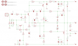
Final schematic...
Hi guys
I did some more work on my latfet version this morning, tidying up a few things and putting some safety diodes across the ground lift.
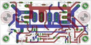
With the layout roughed out, I can see what board space is available for component optimisation.
I'm keen to maximise the voltage swing into the output stage, since this circuit has been designed to run from relatively low rails (35-45V), and the MOSFET outputs will require significantly more gate drive to saturate than the BJT version.
The -ve side is already taken care of due to the action of the bootstrap, but we can do better with the +ve. To that end I've added a switching diode to the +ve rail to stop the output stealing current from input stage under load.
I'm also worried about the Vdrop incurred from the heavy RC filter so I've reduced R18 from 100R to 10R and increased C11 from 100u to 1m to compensate.
I now consider this schematic "final" unless someone finds an error, or some kind soul is able to model this in Spice and supply optimised values.
Is anybody able to comment on the board layout? I'd like to get this finalised in the next couple of days and off to the board house 🙂
Hi guys
I did some more work on my latfet version this morning, tidying up a few things and putting some safety diodes across the ground lift.
With the layout roughed out, I can see what board space is available for component optimisation.
I'm keen to maximise the voltage swing into the output stage, since this circuit has been designed to run from relatively low rails (35-45V), and the MOSFET outputs will require significantly more gate drive to saturate than the BJT version.
The -ve side is already taken care of due to the action of the bootstrap, but we can do better with the +ve. To that end I've added a switching diode to the +ve rail to stop the output stealing current from input stage under load.
I'm also worried about the Vdrop incurred from the heavy RC filter so I've reduced R18 from 100R to 10R and increased C11 from 100u to 1m to compensate.
I now consider this schematic "final" unless someone finds an error, or some kind soul is able to model this in Spice and supply optimised values.
Is anybody able to comment on the board layout? I'd like to get this finalised in the next couple of days and off to the board house 🙂
Attachments
Are the catch diodes actually included in the output devices? Actually, the gate zener and diode is included as well on the Renesas datasheet.
You could simplify the board a little more, it's a good layout.
The technical issue is how much the output offset will move around with temperature; you might need to consider thermally isolate the Vbe multiplier so it tracks only the input device, which of course is cool, runs below 50mW.
Hugh
You could simplify the board a little more, it's a good layout.
The technical issue is how much the output offset will move around with temperature; you might need to consider thermally isolate the Vbe multiplier so it tracks only the input device, which of course is cool, runs below 50mW.
Hugh
Last edited:
Member
Joined 2009
Paid Member
Thank you gentlemen, I checked the Renesas schematic for myself and you are quite correct. I'll update the files when I get home tonight.
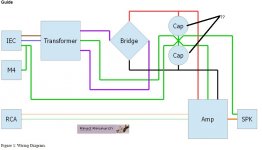
Sorry to hijack the R&D flavour of this thread, but I'm just finishing up the wiring of my TGM8 (original version) and have used the attached diagram (courtesy of DIYAUDIO member richie00boy) as a layout reference.
Is anyone able to advise what value (voltage + uF) capacitors in the diagram would be suitable for 35vdc post-rectified supply? Also - what is the actual purpose of these capacitors?
Is anyone able to advise what value (voltage + uF) capacitors in the diagram would be suitable for 35vdc post-rectified supply? Also - what is the actual purpose of these capacitors?
Attachments
Member
Joined 2009
Paid Member
These capacitors filter the charge pulses coming off the rectifier, acting as integrators to provide a smoother d.c. voltage to the amplifier. They also provide a return path for signal current returning from the speaker ground connection back to the bridge rectifier.
Depending on your transformer the voltage may be higher than 35V as the circuit draws little current in idle. Some transformers will give you 10% extra voltage when not under load. You'll likely be safest with 50V rated caps and since it's a popular voltage rating there should be lots of options.
Depending on how much capacitance you have on the amplifier board - the pcb I used has enough capacitance that it's not necessary to add any off-board. I used a 4,700uF cap, then an 0R33 resistor and then another 4,700uF cap per rail; thus providing some CRC ripple filtration. You could likely get good results with less capacitance (maybe half of what I used) and you could also use more capacitance (e.g. double).
Last edited:

Member
Joined 2009
Paid Member
You have the fancy blue boards - good for you !
The wiring diagram looks fine. But wait a minute..
Did you check everything on the pcb is fitted properly ?
Where is the safety earth connected to the metal chassis ? - I recommend that the safety earth from the IEC goes to the chassis. The amplifier signal ground / speaker ground all connect together near the amplifier and then a single wire goes from there to to the chassis via a pair of diodes wired in parallel but in opposite directions to isolate the signal ground from the noisy mains ground - helps reduce hum.
Can you power up slowly with a variac, or with a light bulb in series with the mains supply ? - these are standard precautions for a new build.
At your lower power rail voltages (TGM8 was designed for 50V, although I use 42V) you may need to adjust a resistor value to ensure the dc-offset circuit has enough range for adjustment (there is some discussion around post 200) - which version did you build - the full version with enhanced VAS ?
Last edited:
Member
Joined 2009
Paid Member
The amplifier signal ground / speaker ground all connect together near the amplifier and then a single wire goes from there to to the chassis via a pair of diodes wired in parallel but in opposite directions to isolate the signal ground from the noisy mains ground - helps reduce hum.
p.s. don't use small signal diodes for this ground-break circuit, you want something beefy enough to hold up under a fault condition - use rectifier diodes, or a spare bridge rectifier (Nelson Pass recommendation).
p.p.s. another precaution is the output idle current, the bias. You don't want to start off with a high bias or you'll get rapid heating of the output devices - be ready to turn the bias (incorrectly labelled as offset on the original pcb) down.
Sorry for the ad-hoc advice here, if Ranchu (Christian) is available you could ask him for some help, he's in your time zone at least and knowing how helpful he is, he might be able to offer some better guidance by phone than I can over the forum here.
Last edited:
If you have a multimeter handy it would be worthwhile testing the polarities of the DC from the bridge rectifier before plugging it into the amp board. If the wires are swapped you'll blow fuses (or worse!).
Gareth, I trimmed the DC offset and bias on these boards for lordearl's target 35VDC rails, prior shipping so they should be literally "plug and play".
You have the fancy blue boards - good for you !
The wiring diagram looks fine. But wait a minute..
Did you check everything on the pcb is fitted properly ?
Where is the safety earth connected to the metal chassis ? - I recommend that the safety earth from the IEC goes to the chassis. The amplifier signal ground / speaker ground all connect together near the amplifier and then a single wire goes from there to to the chassis via a pair of diodes wired in parallel but in opposite directions to isolate the signal ground from the noisy mains ground - helps reduce hum.
Can you power up slowly with a variac, or with a light bulb in series with the mains supply ? - these are standard precautions for a new build.
At your lower power rail voltages (TGM8 was designed for 50V, although I use 42V) you may need to adjust a resistor value to ensure the dc-offset circuit has enough range for adjustment (there is some discussion around post 200) - which version did you build - the full version with enhanced VAS ?
Yes, the nice blue ones! And Christian (Ranchu32) populated the boards and tested/adjusted dc offset w/ 35v rails, so it should be OK from that perspective.
I don't have a variac, but can certainly wire the amp in series with a light bulb.
Re the ground, I drilled the ground hole about 15cm away from the IEC socket on the base panel on the chassis, and have it connected via a lug to the IEC socket, the centre tap of the transformer, the speaker GND and the GND from the PCB.
So it would appear that the distance from the IEC socket to the star/chassis ground is OK, I just need to remove the 'other grounds' (speaker, pcb, centre tap) and solder a pair of diodes between the chassis ground and the 'other grounds'. As attached?
Attachments

p.s. don't use small signal diodes for this ground-break circuit, you want something beefy enough to hold up under a fault condition - use rectifier diodes, or a spare bridge rectifier (Nelson Pass recommendation).
OK. All I have at this stage is a W04 1.5A 400V Bridge Rectifier, which might not be suitable.
Can you recommend something from the Jaycar diode catalogue here which won't necessite the drilling of another hole (I've busted about 6 drill bits getting the current chassis into shape!!)?
Member
Joined 2009
Paid Member
For now you can keep all the grounds connected at the chassis - at least to test out the amplifier. The diodes are helpful if you have ground loops that create hum. You might not get any hum.
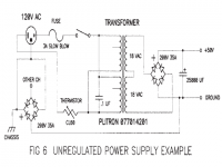
The bridge rectifier you have can be used to break the ground loops, no need to buy any new parts unless you prefer to. I don't know if this makes sense, but I've attached a diagram drawn by Nelson Pass, part of his Zen Variations 4 article that shows a bridge rectifier being used to separate the chassis ground from the amplifier ground (lower left corner of the diagram).
The bridge rectifier you have can be used to break the ground loops, no need to buy any new parts unless you prefer to. I don't know if this makes sense, but I've attached a diagram drawn by Nelson Pass, part of his Zen Variations 4 article that shows a bridge rectifier being used to separate the chassis ground from the amplifier ground (lower left corner of the diagram).
Attachments
Last edited:
Well the W04 will be simple to wire in, I can glue it with some epoxy to hold it in place, adjacent to the chassis ground. But given there is only two connections to solder (chassis to rectifier, rectifier to signal ground), what is the wiring?
Attachments
Last edited:
Member
Joined 2009
Paid Member
what is the wiring?
I edited my previous post to add a diagram from Nelson Pass (ignore the connection to 'other channel' unless you have dual power suppliers) - does it help ?
Last edited:
- Home
- Amplifiers
- Solid State
- TGM8 - my best amplifier, incredible bass, clear highs, no fatigue (inspired by Rod Elliot P3a)