I've heard elsewhere that ferrites in digital signal lines, like the I2S lines, are not a good idea in that they tend to become magnetized over time.
I don't use ferrite beads in the I2S signal lines but in series with resistors and a 10mH choke that are used to set a reference voltage and connect to +5V. The ferrite bead increases impedance at higher frequencies in order to compensate for the effects of 10mH self capacitance. The idea is to create a high series impedance to the power supply (mainly passing DC current) in order to prevent I2S signals from polluting the 5V power supply.
What are your recommendations for I2S attenuators for I2S signals when feeding OS (digital filtering) ICs. E.g., lines from decoder to DF (e.g. SAA7210 --> SAA7220)?
Jitter on SAA7220 DF output is very high, all I2S signals must be synchronously reclocked prior to feeding these to the TDA1541A. The I2S attenuators reduce TDA1541A I2S input circuit ground-bounce and have little to do with the I2S source.
My clock is a Kwack Clock v7.
Here are some weak points of the Kwak clock:
Poor PSRR of the Colpitts oscillator (typical power supply-induced frequency fluctuation equals 20Hz / volt).
The comparator input (clock load) will induce frequency shift (jitter) using this application, estimated dynamic frequency deviation equals at least 40Hz.
With a perfect reference voltage (zero noise) the comparator still adds significant jitter.
Highly critical comparator reference voltage circuit, the slightest noise on the reference input will translate to increased jitter.
Noise levels of voltage regulators are still way too high in order to achieve low jitter with given Colpitts oscillator poor PSRR. Unfiltered TL431 noise spectrum is also pretty fatal here. ferrite beads won't offer any significant attenuation of both mains borne and TL431 noise.
(ecdesigns: did you ever post a schematic on your 4V clock?)
I didn't post schematics of my 3-crystal master clock yet.
Is your set-up OS or NOS?
My setup is NOS without any (analogue) filtering at all. I use large bandwidth signal processing all the way up to the speaker chassis. Required Brickwall filtering (Nyquist–Shannon sampling theorem) is done by the human auditory system that has a sharp cut-off frequency of around 20KHz.
I use a SD-transport for digital audio source, and a selected cryo-treated TDA1543 with passive I/V conversion (no semiconductors in the signal path). I use one hybrid output coupling cap.
Volume control is passive (10K ALPS/TDK stereo pot).
Active amplification is done using discrete, balanced, zero global feedback, very high resolution, fully DC-coupled all-FET bridge amps. I only use 6 FETs / channel for active amplification.
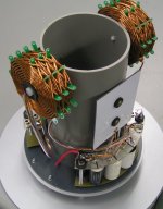
The speakers are semi 2-way omni-directional systems with very high resolution passive crossovers, and a third internal speaker that acts as corrective element (magneto-dynamic correction loop) and as acoustically driven subwoofer. Efficiency is better than 100dB (1W / 1m).
Passive crossover filters consist of two home-made multi-segmented honeycomb air core chokes, based on home-made 12 x 0.4mm litz wire, and two hybrid caps. Crossover frequency equals 5 KHz. Filters are second order (12dB / octave).
I attached a photograph showing this passive crossover.
Attachments
.....
Here are some weak points of the Kwak clock:
Poor PSRR of the Colpitts oscillator (typical power supply-induced frequency fluctuation equals 20Hz / volt).
The comparator input (clock load) will induce frequency shift (jitter) using this application, estimated dynamic frequency deviation equals at least 40Hz.
With a perfect reference voltage (zero noise) the comparator still adds significant jitter.
Highly critical comparator reference voltage circuit, the slightest noise on the reference input will translate to increased jitter.
Noise levels of voltage regulators are still way too high in order to achieve low jitter with given Colpitts oscillator poor PSRR. Unfiltered TL431 noise spectrum is also pretty fatal here. ferrite beads won't offer any significant attenuation of both mains borne and TL431 noise.
I didn't post schematics of my 3-crystal master clock yet.
......
If noise is of such paramount importance how can it be that the Supertubeclock as used in the PrimaLuna Prologue 8 CDP has received such rave reviews from all over the world?
Either concept must be wrong. The triode tube in the Supertubeclock is noisy almost by definition.

See also:
http://www.diyhifi.org/forums/viewtopic.php?f=2&t=1284&hilit=supertubeclock
Last edited:
this will introduce more jitterI used a low distortion sine wave source to clock the flip flop
RCThe required resistors for the LC filters are integrated in the TDA1541A chip.
DEM syncing with input data would remove statistical average, so with a good pcb layout(tracing) and capacitors with low leakage, low ESR, ESL and impedance(1-10u 1206 X7R) standard asynchronous solution sounds better.
These capacitors should have the following requirements:Any personal suggestions here for values and/or types?
1 minimum impedanse (and minimum ESR, ESL).
2 minimum leakage.
3 minimum dimensions and physically located under the 1541 body (smaller "EMI fishing").
In practice - capacity of not less than 1u, dimensions not more than SMD 1206
this will introduce more jitter
This depends on the application, both square (ground-bounce) and sine wave (trigger uncertainty) signal injection increase jitter and affect jitter spectrum. The trick is to determine the lesser of these two evils. I had slightly better performance with injecting a low distortion 10Vpp sinewave using capacitive coupling (0.5pF) and a suitable bias voltage at the flip flip clock input.
DEM syncing with input data would remove statistical average, so with a good pcb layout(tracing) and capacitors with low leakage, low ESR, ESL and impedance(1-10u 1206 X7R) standard asynchronous solution sounds better.
Asynchronous DEM clock would introduce a second clock source in the system. Since there is on-chip crosstalk between both DEM clock and bit clock (BCK), inter-modulation between these two frequencies will occur. Other problem is that the DEM oscillator has significant DATA induced jitter (frequency fluctuates with I2S DATA pattern). I doubt if external filter caps can prevent increased timing jitter at the output latch that is a result of this inter-modulation.
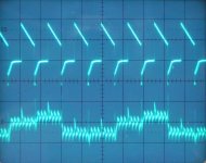
I attached an oscillogram showing typical asynchronous DEM clock during playback (upper picture), and synchronous DEM clock during playback (lower picture).
I also attached an oscillogram of an unfiltered active divider output (decoupling cap removed). The BCK crosstalk is clearly visible (DEM clock rate equals 352.8 KHz here. The stair-case signal is caused by tolerances in the passive divider that drives the time averaging matrix. First two passive divider outputs match quite good, but number 3 and 4 (active divider has 4 outputs) show significant tolerances.
Higher active divider decoupling capacitor values will increase peak currents. Increasing DEM clock rate (works up to approx. 2.8224 MHz) may affect settling time in the time averaging matrix.
The trick is to use optimal synchronous DEM clock rate, and optimal active divider decoupling caps.
Attachments

Please excuse me! I do not speak English. Just read a little. I write with the help of Google translate. Please see the following schematic diagram. Make a DAC for my transport Philips CDD882. S/PDIF is removed. Will use only I2S. Do you see any errors or incorrect logic, please tell me. I've used things from the posts of -ecdesigns- and other. I'd be happy if -ecdesigns-write a comment. Thank you all!
Attachments
I forgot to write what decoupling caps use:
220nF - Stacked Metallized PPS Film Chip Capacitor - ECHU1H224GC9.
I chose 220nF because use and NOS. In this mode, i think 100nF are too small value. But I do not know whether 220nF is good when used 2.8224 MHz DEM reclocking.
PANASONIC|ECHU1H224GC9|CAPACITOR, 2416, 220NF, 50V | Farnell United Kingdom
yes yes, ground is everything...This depends on the application, both square (ground-bounce) and sine wave (trigger uncertainty) signal injection increase jitter and affect jitter spectrum. The trick is to determine the lesser of these two evils. I had slightly better perfo
forget it, use good decoupling, and statistical averaging help get you the best sound😉Asynchronous DEM clock would introduce a second clock source in the system. Since there is on-chip crosstalk between both DEM clock and bit clock (BCK), inter-modulation between these two frequencies will occur.
no-noOther problem is that the DEM oscillator has significant DATA induced jitter (frequency fluctuates with I2S DATA pattern).
somsing wrong with you asynchronous DEMI attached an oscillogram showing typical asynchronous DEM clock during playback (upper picture), and synchronous DEM clock during playback (lower picture).
read the
"Dynamic Element Matching for High Acuracy Monolithic DAC" RUDY J. VAN DE PLASSCHE. IEEE JOURNAL OF SOLID-STATE CIRCUITS, VOL. SC-11, NO. 6, DEC 1976
"A Monolithic 14-Bit D/A Converter" RUDY J. VAN DE PLASSCHE , DICK GOEDHARD. IEEE JOURNAL OF SOLID-STATE CIRCUITS, VOL. SC-14, NO. 3, JUNE 1979
"A Monolithic Dual 16-Bit D/A Converter" HANS J. SCHOUWENAARS, EISE CAREL DIJKMANS, BEN M. J. KUP, AND ED J. M. VAN TUIJL. IEEE JOURNAL OF SOLID-STATE CIRCUITS, VOL. SC-21, NO. 3, JUNE 1986.
www.diyaudio.org.ua/viewtopic.php?f=20&t=205
I'd be happy if -ecdesigns-write a comment. Thank you all!
Choke (10mH) also required in series with each 3K3 resistor that connects to +5V.
Thank you -ecdesigns- !Choke (10mH) also required in series with each 3K3 resistor that connects to +5V.
But when using 220 nF decoupling caps, better is it to be DEM clock is 352.8 or 176.4 KHz ?
Thank you -ecdesigns- !
But when using 220 nF decoupling caps, better is it to be DEM clock is 352.8 or 176.4 KHz ?
I have better sound with 358.2khz.
What is yours?
Can you post your working re-clock circuit?
Already post (post#166). But I do not have a working version. I think changing the schеmatic with 358.2kHz DEM reclocking (like you). I finished with simulations of the clock circuit and psu. When I do making PCB I will continue to DEM. Post schematic if anyone is interested. Can you post your 358.2kHz re-clock circuit? Тhank you!I have better sound with 358.2khz.
What is yours?
Can you post your working re-clock circuit?
Attachments
Already post (post#166). But I do not have a working version. I think changing the schеmatic with 358.2kHz DEM reclocking (like you). I finished with simulations of the clock circuit and psu. When I do making PCB I will continue to DEM. Post schematic if anyone is interested. Can you post your 358.2kHz re-clock circuit? Тhank you!
Hi,
I'm also trying to build a DEM reclocking circuit. At first I built Henk ten Pierick's circuit (first page of this thread), but it didn't work too well, so I started searching for another circuit. I found it
 here (post #34). I built it slightly different, but the results are the same. I will find a circuit-draw program tomorrow and upload my schematics, but only if it works of course😉
Kind regards,
Joris
I will be happy to see your schematic diagram🙂...I will find a circuit-draw program tomorrow and upload my schematics, but only if it works of course😉
Kind regards,
Joris
Hi,
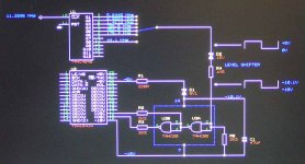
Here is my schematic.
I built it with reference to -ecdesigns- circuit, he's the one who set the
basic setup for this circuit. All the credits go to him.
Instead of taking the -5v power line into a resistor and a zener diode I decided to use a 7805 voltage regulator. This ensures that the 74HC74's will not cause noise on the power lines. The circuit is pretty sensitive for noise in the environment, so copper shielding the whole pcb is a pretty good idea.
Also use of shielded cable to connect the pcb to pin 16 and 17 is usefull.
The input of the 74HC4040 is connected to a clock source, in most cases that clock is 11.2896 MHz, in some cases it is 12.2880 MHz, the DEM frequency will increase to 384 KHz, this isn't a problem. I haven't tried what the maximum DEM frequency is yet. I can't guarantee that a sampling frequency of 96 KHz will work, this will result in a DEM frequency of 768 KHz.
Kind regards,
Joris Colijn
Attachments
Hi,
Here is my schematic.
I built it with reference to -ecdesigns- circuit, he's the one who set the
basic setup for this circuit. All the credits go to him.
Instead of taking the -5v power line into a resistor and a zener diode I decided to use a 7805 voltage regulator. This ensures that the 74HC74's will not cause noise on the power lines. The circuit is pretty sensitive for noise in the environment, so copper shielding the whole pcb is a pretty good idea.
Also use of shielded cable to connect the pcb to pin 16 and 17 is usefull.
The input of the 74HC4040 is connected to a clock source, in most cases that clock is 11.2896 MHz, in some cases it is 12.2880 MHz, the DEM frequency will increase to 384 KHz, this isn't a problem. I haven't tried what the maximum DEM frequency is yet. I can't guarantee that a sampling frequency of 96 KHz will work, this will result in a DEM frequency of 768 KHz.
Kind regards,
Joris Colijn
Refer to EC's circuit R3, 4, 5, 6 should be 10K.
2K2 goes to -15V in oder to stop the internal clock.
Hi fastvideo,
I guess you have a different schematic. It sounds quite reasonable to connect the outputs through a resistor to -15v, but that is when the inverter outputs signals referenced to the ground. In this circuit, the signals are referenced to -15v already, so the connection to the -15v hasn't got to be made. The circuit works very well after a few tries, is it possible to increase the DEM frequency to 706,5 KHz? I'm willing to rewire the pcb, but I don't want to destroy my 2 TDA1541A's...
I must admit, after listening for some time, I noticed that there is better detail retrieval and tighter bass. This modification was worth the effort after all!
I attached the schematic EC drew.
Kind regards,
Joris
Attachments
Hi fastvideo,
I guess you have a different schematic. It sounds quite reasonable to connect the outputs through a resistor to -15v, but that is when the inverter outputs signals referenced to the ground. In this circuit, the signals are referenced to -15v already, so the connection to the -15v hasn't got to be made. The circuit works very well after a few tries, is it possible to increase the DEM frequency to 706,5 KHz? I'm willing to rewire the pcb, but I don't want to destroy my 2 TDA1541A's...
I must admit, after listening for some time, I noticed that there is better detail retrieval and tighter bass. This modification was worth the effort after all!
I attached the schematic EC drew.
Kind regards,
Joris
Sorry for the mistake. This is the first circuit i have tested, but it doesn't work well with me. http://www.diyaudio.com/forums/digital-line-level/146841-4xtda1541a-nos-dac-project-7.html#65
Sorry for the mistake. This is the first circuit i have tested, but it doesn't work well with me. http://www.diyaudio.com/forums/digital-line-level/146841-4xtda1541a-nos-dac-project-7.html#65
My working circuit: #3062
http://www.diyaudio.com/forums/digital-line-level/79452-building-ultimate-nos-dac-using-tda1541a-307.html
- Home
- Source & Line
- Digital Line Level
- TDA1541 DEM reclocking