2) Use discrete voltage regulators for +5V, -5V, and -15V, LM78xx, LM79xx, LM317, LM337, and TL431-based regulators aren't suitable for this application and cause significant sound quality degradation.
I could post some schematics of suitable regulators.
I'm curious for the schematics, thank you!
I'm curious for the schematics, thank you!
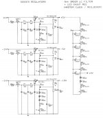
I attached schematics for +5V, -5V, and -15V series regulator (TDA1541A) and a LED shunt regulator for powering a masterclock and or reclocker.
Series regulators:
The input voltage is first filtered (N1, N2, C1, R1, C2), then fed to the basis of a darlington transistor that is used for series regulation.
L1, N3, N4, and C4 form a filtered LED reference of approx. 2V. Bandgap references produce much more noise compared to a suitable LED reference, thats why I used a LED here. I used a green LED because these have highest voltage drop (approx. 2V) and offer low noise. The noise of this reference LED is filtered through a LC filter. I put a ferrite bead (MURATA filter) in series with the 10mH choke in order to reduce the effects of 10mH choke self capacitance. Its even better to split-up the 10mH choke in multiple lower value chokes in series (3 x 3.3mH for example), this places the chokes self capacitances in series, further lowering self capacitance of this hybrid choke.
The output voltage is divided (R3, R4) and fed to the basis of T2. The emitter of T2 sits on the 2V LED reference, and when the output voltage exceeds 2V + Vbe (approx. 0.6V) it starts to conduct and reduces the current flow through T1 by lowering its basis current. This way the output voltage is stabilized. Fine tuning of the output voltage can be done by slightly varying the value of R3. C3 is added for stability (the circuit may oscillate without this cap).
I kept the feedback loop simple and straight-forward in order to improve feedback loop dynamic properties. This is important when powering highly sensitive loads like analogue circuits and DACs.
The other two regulators (-5V and -15V) are based on the same circuit. The -15V regulator has a 6V LED reference in order to reduce the effect of amplifying LED reference noise.
Shunt regulator:
I also attached a schematic of a filtered LED shunt regulator, fed by a 9th order LC hybrid filter. This filter significantly attenuates the already low noise output voltage of the series reg, it also increases series impedance between polluted mains power supply and loads.
Other important factor is that the LED itself is the regulator, meaning there is no feedback loop. This provides better dynamic properties.
Maximum output current depends on choke DC resistance and max. LED current.
Attachments
Last edited:
since I try to learn about reclocking I would be thankful to point me to some reclocking schematic - some simple and effective
With reclocking there are two major issues, first is getting both clocks in one time domain, this is easiest by using a common master clock for both source and DAC.
Next issue is reducing master clock frequency to the required timing frequency signal (BCK for TDA154x) while retaining lowest possible jitter.
If all logic building blocks like gates and flip-flops for example were perfect, this would be peanuts, however, in practice each of these building blocks introduce problems like ground-bounce, jitter, propagation delays and issues with exact moment of triggering.
This means that when you derive BCK from the master clock, you would need multiple flip-flops. Multiple cascaded flip flops introduce more ground-bounce, jitter and trigger issues compared to a single flip flop.
Therefore its easier to achieve better results using synchronous reclocking, requiring only a single flip-flop. In this case the BCK signal generated by the source is synchronously reclocked using a single flip flop.
In order to maintain low jitter, the flip flop used for synchronous reclocking must be powered by an ultra low noise regulator, similar as required for the master clock. In practice this highly critical flip flop is simply connected to a polluted 5V supply, boosting jitter significantly.
next big problem is ground bounce, when using a neat square wave clock signal with fast transients, the flip flop input circuit (data and clock) will be flooded with unwanted HF energy, resulting in significantly increased ground bounce and resulting increased jitter levels.
In order to visualize the effect of ground bounce, imagine a capacitor being charged or discharged very rapidly, this will induce surge currents, these surge currents will produce unwanted voltage drops across conductors that don't have infinitely low impedance. These surge currents increase with switching frequency, transients, and voltage. So ground-bounce can be reduced using slower transients, lower switching frequency and lower supply voltages.
I used a low distortion sine wave source to clock the flip flop. The clock input was set to a bias voltage of half the power supply voltage, and the sine wave was injected through 0.5 ... 1pF coupling cap. The other circuits (SD transport) were connected trough a discrete commplementary clock buffer.
Other problem, often overlooked is grounding, in order to get accurate triggering its handy to have at least one stable reference (GND). Unfortunately this GND reference often shares currents with other circuits. As a result of this, noise will be injected into the GND routes as they don't have infinite low impedance. Plain PCB GND traces are very thin and impedance usually isn't low enough. I had to use thick home-made litz wire (128 x 0.2mm laquered copper wire twisted together) in order to reduce GND trace impedance to acceptable levels.
as I see there Is two reclock types used - 1 reclocking I2S - BCK, WS, data;
2 DEM reclocking TDA1541 pin 16 and 17
For the TDA1541A, BCK is used for sample timing, so BCK must have lowest jitter and needs to be reclocked. reclocking WS and DATA means making a compromise, there are more clock loads that will affect master clock jitter performance, and there is the risk of crosstalk between WS, DATA and the master clock. After extensive tests, I decided not to reclock WS and DATA signals.
The TDA1541A uses a DEM clock for the Dynamic Element matching circuit, this circuit could be compared with a circuit that constantly calibrates the 6 MSBs. In order to do so it averages 4 input currents, this is done using so called active dividers, these both divide and average these input currents. The idea is to end up with 16 binary weighted precision currents. The DAC analogue output is then connected to combinations of these current sources by means of diode-transistor bit switches.
The 14 decoupling capacitors required for the TDA1541A, filter the outputs of the active divider circuits. Note that the active divider output currents are static. The required resistors for the LC filters are integrated in the TDA1541A chip. The filter caps must offer low enough impedance up to 200 KHz signals, so bulky audiophile or large film caps are less suitable for this task. However, its very important that these filter caps have low DC leakage current, otherwise this will lead to bit errors as the active divider output currents will now be split between DAC output and filter cap leakage current. Also note that PCBs can introduce leakage currents too (contamination in combination with moisture on the PCB). So the PCB must be kept as dry and clean as possible.
can you confirm that this circuit TDA1541 DEM reclocking will work
The DEM clock part will work, except jitter will be rather high (counter plus inverter). I would synchronously reclock the divider output using a flip flop that provides both inverted and non-inverted DEM clock.
BCK clock frequency depends on the configuration. If I am correct the SAA7220 uses 32 bits / frame, thus BCK frequency needs to be 44,100 * 32 = 1.411,200 MHz for NOS (master clock divided by 8) and 44,100 * 32 * 4 = 5.6448 MHz for 4 x OS (master clock divided by 2).
The dividers in the schematic will add more jitter compared to a single flip flop. I would use a single D flip flop (inverted Q output fed back to the data input) as divide by 2 circuit for OS.
For NOS I would use a divider (divide by 8) followed by a synchronous reclocker.
here are suitable single flip flops (SMD) for reclocking:
STMICROELECTRONICS|74V1G80CTR|LOGIC, 74V1G, D-TYPE FLIP-FLOP | Farnell Nederland
STMICROELECTRONICS|74V1G79CTR|LOGIC, 74V1G, D-TYPE FLIP-FLOP | Farnell Nederland
Hi EC,
Thank you for all this help. I am happy with the result with the dem reclock.
Is there any difference on performance?
One inject signals though capacitors.
The other inject signals directly.
Thank you for all this help. I am happy with the result with the dem reclock.
Is there any difference on performance?
One inject signals though capacitors.
The other inject signals directly.
Last edited:
Is there any difference on performance?
Yes there is a difference,
The DEM clock needs to have low jitter and induce lowest possible crosstalk. The problem is that the DEM clock needs to be injected in an on-chip oscillator that must not be allowed to oscillate.
The DEM clock has direct effect on the bit errors of the 6 MSBs in the TDA1541A, and on-chip crosstalk (inter modulation between DEM clock and other on-chip clocks) thats why there are clearly audible differences between DEM clock circuits.
I noticed that the indicated 200KHz DEM clock causes a number of issues like problems with active divider settling time, crosstalk with on-chip clock signals, ground-bounce, and problems with external decoupling film caps (inductance).
Other problems are the extra divider and inverter required to derive the DEM clocks that add jitter (every logic element adds jitter). The DEM clock distribution among multiple TDA1541A chips is also problematic.
So I tried to design a simple but highly effective DEM clock injection circuit that uses one of the local I2S signals.
After some experimenting I decided to use the WS signal (44.1 KHz). Decoupling cap value can be increased to approx. 400nF (390nF) in order to achieve similar filter characteristics although 100nF worked fine too.
WS was connected to the anode of a Schottky diode, the cathode was connected to a resistor of exactly 13K, and the resistor was connected to pin 16. Pin 17 was left unconnected.
The value of 13K corresponds with a WS signal amplitude of exactly 3.3V (SD-transport I2S output level). The value needs to be increased to 14 ... 15K when when using 5V signal level. The value of the resistor is critical, too high tolerance will prevent the on-chip DEM clock from tracking. This method uses current steering, so the current deviations must be tuned in such way that the DEM oscillator tracks reliably.
This circuit worked best so far, but one needs to verify that it works correctly before drawing any conclusions. Correct operation can be checked by temporarily removing one of the 14 active divider bypass caps and measuring the signal on this pin. If the DEM circuit works correct, there must be a stair case signal that runs in sync with WS, if not, resistor value needs to be fine tuned (trimmer could be used to determine exact value).
When using multiple TDA1541A chips, simply repeat this circuit (diode plus resistor) for each TDA1541A chip.
Other method is connecting pin 16 to -15V through a 2K2 resistor, and pin 17 to -15V using a 2K2 resistor. The DEM signal can then be injected using 10K Ohm between inverted and non-inverted DEM clock (5V) and pin 16, and inverted DEM clock (5V) and pin 17.
One could also experiment with DEM clock injection (non-inverted clock on pin 16, inverted clock on pin 17) through capacitors. The 2K2 resistors must be left in place in order to prevent the on-chip DEM oscillator from oscillating.
Last edited:
Could a small 1:1 transformer be used for coupling the DEM clock signal? The primary could be fed from the sync reclocker flip-flop, the secondary (floating) between pin 16 and pin 17.
Thx for the detailed write-up!I attached schematics for +5V, -5V, and -15V series regulator (TDA1541A) and a LED shunt regulator for powering a masterclock and or reclocker.
I noticed you use monolithic Darlingtons BD679/80 in a traditional Darlington set-up. What's the advantage here over a straight-up Darlington (links to other posts or threads may be helpful)?
On the shunt reg...Why choose shunt over series for master clock and reclocker?
I've seen a lot of DIY and commercial-brand variety for these caps. On the commercial side, Philips, of course, used SMD ceramics for the most part. Weirdly, the TDA1541A datasheet values are diff. from a Philips CDP schematic value: 100nF and 220nF, respectively. Any personal suggestions here for values and/or types?The 14 decoupling capacitors required for the TDA1541A, filter the outputs of the active divider circuits.
About that "+4V" output value on the LED shunt regulator for powering a masterclock and or reclocker ... I assume you chose 4V as a convenient middle ground between 3.3 and 5V?
Finally ... to work most efficiently, how much voltage headroom should the pre-regulator provide for the series and shunt topologies you use? E.g., Vin = -20V for the -15V reg., Vin = -10V for the -5V reg., etc.
Last edited:
I noticed you use monolithic Darlingtons BD679/80 in a traditional Darlington set-up. What's the advantage here over a straight-up Darlington (links to other posts or threads may be helpful)?
I just used these to create a compact design (fewer parts). It's also possible to use Darlingtons constructed with discrete components in these voltage regulators of course.
On the shunt reg...Why choose shunt over series for master clock and reclocker?
I first use a series regulator to achieve a stabilized low noise 5V power supply, next I use a 9th order lowpass that feeds a filtered LED shunt regulator.
Series regulators require feedback loops, and the feedback loop activity becomes audible with ultra low jitter master clocks and especially the reclocker. The LED shunt regs I use have no feedback loop.
The LED shunt creates a low noise voltage that is then LC filtered. It also provides the required reference voltage for the reclocker. This shunt regulator concept has provided best results for this specific application.
've seen a lot of DIY and commercial-brand variety for these caps. On the commercial side, Philips, of course, used SMD ceramics for the most part. Weirdly, the TDA1541A datasheet values are diff. from a Philips CDP schematic value: 100nF and 220nF, respectively. Any personal suggestions here for values and/or types?
Don't use ceramic caps as these suffer from piezoelectric effects, if you have to use these, always use NPO types.
When using film caps, use versions with stacked construction (SMD film) for obtaining lowest inductance. Polyester capacitors and capacitors made with comparable dielectric will be fine. The bulky polypropylene caps have too high inductance, suffer from foil resonances, and require too long PCB traces to be effective at DEM clock rates of 200 KHz typical.
By lowering the DEM clock frequency to 44.1KHz and increasing decoupling cap value to 390nF, cheap stacked polyester film caps will work very well, and wiring becomes less critical as switching frequency is now much lower. Its also possible to use 4 x 100nF SMD film caps (1206) in parallel.
Also note that no audio signal flows through these active divider decoupling caps. The voltage across the external filter cap is static, this can be easily verified by measuring the voltage across these caps using an oscilloscope.
About that "+4V" output value on the LED shunt regulator for powering a masterclock and or reclocker ... I assume you chose 4V as a convenient middle ground between 3.3 and 5V?
I use a highly optimized discrete super clock (up to 400 times lower jitter compared to audiophile clocks when driving multiple clock loads and running on mains power). These super clocks only make sense when using a virtually perfect digital audio source (I use a semiconductor memory-based SD transport) and highly optimized clock distribution.
This clock offers best performance when running on exactly 4 volts.
The clock uses multiple crystals in series that are used for both, oscillation and primary output signal filtering. This way, low distortion sinewave with high spectral purity is produced for driving the highly sensitive synchronous reclocker.
The secondary output (square wave) is buffered using a complementary choke-loaded buffer. The complementary buffers are designed to offer very high PSRR and maximize load immunity, super clock frequency remains extremely stable (less than 0.01Hz / pF load fluctuation).
Both conventional and audiophile clock frequency changes up to 20Hz / Volt power supply fluctuation, that's why the ultra low noise power supplies are essential, these are often integrated with the master clock.
The clock frequency also varies up to 2Hz / pF dynamic load capacity fluctuation (clock buffers and comparators form the first clock load, and induce these frequency shifts). Extra frequency shift can be induced by loads connected to integrated clock buffer or comparator.
I tap a 2V reference voltage from the LED shunt (I use a separate filter for each LED) for setting the bias voltage for the synchronous reclocker. The 10Vpp sine wave from the super clock is injected through 0.5pF capacitive coupling (this ensures max. 0.005Hz load-dependent clock frequency fluctuation). I don't use a square wave here because I need to achieve maximum spectral purity.
The 2V bias voltage is supplied to the synchronous reclocker using a 5 K Ohm bulk metal foil resistor. This way I achieve highly accurate triggering without using an extra comparator that adds jitter. I also minimize ground-bounce in the reclocker input circuit this way.
Both master clock and reclocker share the same 4V ultra low noise supply, maximizing trigger accuracy.
The other clock load (processor) is connected to the super clock secondary buffered clock output.
Finally ... to work most efficiently, how much voltage headroom should the pre-regulator provide for the series and shunt topologies you use? E.g., Vin = -20V for the -15V reg., Vin = -10V for the -5V reg., etc.
Depending on unregulated power supply ripple voltage, headroom needs to be around around 5V. So +10V, -10V, and -20V unregulated input voltage for +5V, -5V, and -15V respectively.
TDA1541 bypass caps; regulator heat; etc.
ecdesigns... WOW! What an informative, exhaustive response!
One thing about your regulator set-up I forgot to ask about was heat.
The 1541 and other classic Philips ICs, like the SAA7210 and SAA7220, are current hogs. The chips run quite warm as a result. Are you heat-sinking any component in your series/shunt regulator -- e.g., BD679/80, perhaps?
IAC, I may build your series/shunt regulator module and may wish to power the 200mA-drawing SAA7210 and SAA7220. Any suggestions here?
There's a topical thread on diyhifi.org here: MKS or MKP use for decoupling cap TDA1541
Perhaps you have something to add.
Thx!
ecdesigns... WOW! What an informative, exhaustive response!
One thing about your regulator set-up I forgot to ask about was heat.
The 1541 and other classic Philips ICs, like the SAA7210 and SAA7220, are current hogs. The chips run quite warm as a result. Are you heat-sinking any component in your series/shunt regulator -- e.g., BD679/80, perhaps?
IAC, I may build your series/shunt regulator module and may wish to power the 200mA-drawing SAA7210 and SAA7220. Any suggestions here?
Most of what you've noted is new to me, so thx for the info! I have not tried NPOs, tho' I know of their reputation. I use Wima SMD (size: 1812) PPS (Metallized Polyphenylene-Sulphide). They just barely fit onto pre-existing PCB, but I think they are worth it.Don't use ceramic caps as these suffer from piezoelectric effects, if you have to use these, always use NPO types.
When using film caps, use versions with stacked construction (SMD film) for obtaining lowest inductance. Polyester capacitors and capacitors made with comparable dielectric will be fine. The bulky polypropylene caps have too high inductance, suffer from foil resonances, and require too long PCB traces to be effective at DEM clock rates of 200 KHz typical.
By lowering the DEM clock frequency to 44.1KHz and increasing decoupling cap value to 390nF, cheap stacked polyester film caps will work very well, and wiring becomes less critical as switching frequency is now much lower. Its also possible to use 4 x 100nF SMD film caps (1206) in parallel.
Also note that no audio signal flows through these active divider decoupling caps. The voltage across the external filter cap is static, this can be easily verified by measuring the voltage across these caps using an oscilloscope.
There's a topical thread on diyhifi.org here: MKS or MKP use for decoupling cap TDA1541
Perhaps you have something to add.
Cool! If you've posted the design/schematics of this clock anywhere, can you throw me a link?I use a highly optimized discrete super clock (up to 400 times lower jitter compared to audiophile clocks when driving multiple clock loads and running on mains power).
Thx!
Last edited:
I attached schematics for +5V, -5V, and -15V series regulator (TDA1541A) and a LED shunt regulator for powering a masterclock and or reclocker.
Series regulators:
The input voltage is first filtered (N1, N2, C1, R1, C2), then fed to the basis of a darlington transistor that is used for series regulation.
L1, N3, N4, and C4 form a filtered LED reference of approx. 2V. Bandgap references produce much more noise compared to a suitable LED reference, thats why I used a LED here. I used a green LED because these have highest voltage drop (approx. 2V) and offer low noise. The noise of this reference LED is filtered through a LC filter. I put a ferrite bead (MURATA filter) in series with the 10mH choke in order to reduce the effects of 10mH choke self capacitance. Its even better to split-up the 10mH choke in multiple lower value chokes in series (3 x 3.3mH for example), this places the chokes self capacitances in series, further lowering self capacitance of this hybrid choke.
The output voltage is divided (R3, R4) and fed to the basis of T2. The emitter of T2 sits on the 2V LED reference, and when the output voltage exceeds 2V + Vbe (approx. 0.6V) it starts to conduct and reduces the current flow through T1 by lowering its basis current. This way the output voltage is stabilized. Fine tuning of the output voltage can be done by slightly varying the value of R3. C3 is added for stability (the circuit may oscillate without this cap).
I kept the feedback loop simple and straight-forward in order to improve feedback loop dynamic properties. This is important when powering highly sensitive loads like analogue circuits and DACs.
The other two regulators (-5V and -15V) are based on the same circuit. The -15V regulator has a 6V LED reference in order to reduce the effect of amplifying LED reference noise.
Shunt regulator:
I also attached a schematic of a filtered LED shunt regulator, fed by a 9th order LC hybrid filter. This filter significantly attenuates the already low noise output voltage of the series reg, it also increases series impedance between polluted mains power supply and loads.
Other important factor is that the LED itself is the regulator, meaning there is no feedback loop. This provides better dynamic properties.
Maximum output current depends on choke DC resistance and max. LED current.
Thanks a bunch! I will probably use this for my ad1862 dac digital power supply.
A few questions though:
-what murata choke do you use in this schematic? a farnell link would be nice 🙂
-how do you think this compares to a simple 3 pin regulator (7805/lm317 etc)
-I also like to know if it needs any cooling with the 5v voltage drop
Last edited:
After some experimenting I decided to use the WS signal (44.1 KHz).
I noticed that the indicated 200KHz DEM clock causes a number of issues like problems with active divider settling time, crosstalk with on-chip clock signals, ground-bounce, and problems with external decoupling film caps (inductance).
Other method is connecting pin 16 to -15V through a 2K2 resistor, and pin 17 to -15V using a 2K2 resistor. The DEM signal can then be injected using 10K Ohm between inverted and non-inverted DEM clock (5V) and pin 16, and inverted DEM clock (5V) and pin 17.
I tested with this circuit with 44.1khz, 176.4khz and 352.8khz.
44.1khz, no high and not clear.
176.4khz not enough high and not enough definition.
352.8khz has the best listening result, sound more like playing records.
Last edited:
Hi Fastvideo,
using that scheme you are able to increase the DEM clock frequency right up to 5.6448Mhz - you may not quite get all the way up to this - I settled on 2.8224Mhz with the DEM injection.
Prior to ecdesigns DEM injection using the -15v bias resistors, the highest DEM clock frequency was 352.8khz. Most users experienced distortion with DEM clocks above 352.8khz.
Brad
Hi Fastvideo,
using that scheme you are able to increase the DEM clock frequency right up to 5.6448Mhz - you may not quite get all the way up to this - I settled on 2.8224Mhz with the DEM injection.
Prior to ecdesigns DEM injection using the -15v bias resistors, the highest DEM clock frequency was 352.8khz. Most users experienced distortion with DEM clocks above 352.8khz.
Brad
What is your best listening clock?
hi fastvideo,
I am using a DEM clock frequency of 2.8224Mhz with inverted and non inverted inputs on the DEM clock input pins.
Brad
I am using a DEM clock frequency of 2.8224Mhz with inverted and non inverted inputs on the DEM clock input pins.
Brad
-what murata choke do you use in this schematic? a farnell link would be nice
MURATA|DSS6NZ82A103Q55B|CAPACITOR, 3 TERMINAL, 10000PF | Farnell Nederland
-how do you think this compares to a simple 3 pin regulator (7805/lm317 etc)
This depends on the application, for powering critical analogue circuits, this discrete regulator offers better resolution
-I also like to know if it needs any cooling with the 5v voltage drop
This depends on load current, dissipation in the series transistor equals voltage drop multiplied by the load current. I would advice using a heatsink for currents higher than approx. 100mA @ 5V voltage drop.
ecdesigns
would you please check that schematic
I reclock all I2S data and DEM reclock with quad flip flop 74HC175
If you say that It Is better to not reclock data signal I will disconect that links and connect directly to TDA1541A DACs
also do I need counter with non inverting clock input
regards
would you please check that schematic
I reclock all I2S data and DEM reclock with quad flip flop 74HC175
If you say that It Is better to not reclock data signal I will disconect that links and connect directly to TDA1541A DACs
also do I need counter with non inverting clock input
regards
Attachments
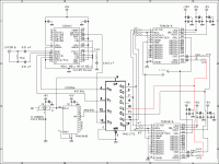
I reclock all I2S data and DEM reclock with quad flip flop 74HC175
Never reclock all I2S signals with one chip, you will get massive crosstalk and highly increased jitter on both BCK and DEM signals. This is also easy to measure using an oscilloscope. The DATA signal causes most problems with crosstalk.
Try to use the single pico gate (SMD) versions, one single flip-flop chip for each signal. use a very clean power supply for both DEM and BCK reclockers.
Always use I2S attenuators for I2S signals when feeding TDA1541A or TDA1543, otherwise you get significant ground-bounce in the DAC chip I2S input circuits, this also increases jitter significantly.
For WS and DATA: 1K from TDA1541A input to GND, 3K3 in series with 10mH choke (3 x 3.3mH in series is even better) and ferrite bead from input to +5V. 3K3 resistor from I2S source to TDA1541A input. The chokes are required to prevent I2S switching noise from polluting the +5V power supply.
For BCK use 330 Ohm and 100 Ohm resistors instead.
thx ecdesigns for your support
I like to ask you if schematic Is correct as a concept for synchronous recloking - any errors from that point
I thought reclocking with single chip Is preferable (perfect synchron, less load to clock)
I will reclock with single flip flops BCK and DEM signal
do you think Is necessary to reclock and WS signal
DATA signal will not be reclocked
do you think that dual TDA1541A will sing better that single
cheers
Ferrites and magnetics
What are your recommendations for I2S attenuators for I2S signals when feeding OS (digital filtering) ICs. E.g., lines from decoder to DF (e.g. SAA7210 --> SAA7220)?
samoloko: Nice job on the schematic. Will you be revising and reposting it soon (per ecdesigns recommendations)? If you do, and keep it updated, it would serve as a nice "reference-grade" topological model for TDA1541 fans 🙂
Here's a good, simple-to-build reclocker that I use. My clock is a Kwack Clock v7. (ecdesigns: did you ever post a schematic on your 4V clock?)Never reclockall I2S signals with one chip, you will get massive crosstalk and highly increased jitter on both BCK and DEM signals. This is also easy to measure using an oscilloscope. The DATA signal causes most problems with crosstalk.
I've heard elsewhere that ferrites in digital signal lines, like the I2S lines, are not a good idea in that they tend to become magnetized over time.Always use I2S attenuators for I2S signals when feeding TDA1541A or TDA1543, otherwise you get significant ground-bounce in the DAC chip I2S input circuits, this also increases jitter significantly.
For WS and DATA: ... and ferrite bead from input to +5V. 3K3 resistor from I2S source to TDA1541A input. The chokes are required to prevent I2S switching noise from polluting the +5V power supply.
What are your recommendations for I2S attenuators for I2S signals when feeding OS (digital filtering) ICs. E.g., lines from decoder to DF (e.g. SAA7210 --> SAA7220)?
samoloko: Nice job on the schematic. Will you be revising and reposting it soon (per ecdesigns recommendations)? If you do, and keep it updated, it would serve as a nice "reference-grade" topological model for TDA1541 fans 🙂
Last edited:
Is your set-up OS or NOS?I am using a DEM clock frequency of 2.8224Mhz with inverted and non inverted inputs on the DEM clock input pins.
- Home
- Source & Line
- Digital Line Level
- TDA1541 DEM reclocking