I think hald the heat here was for you but stayed in France ='(
BTW, can you offer a filter as the one in post 24 but nicely matched for 10K load? Thanks!
BTW, can you offer a filter as the one in post 24 but nicely matched for 10K load? Thanks!
If you did want to include a volume control it wouldn't be a great idea to do it that way inside the DAC. For the reason that the output impedance via the pot is too high to bear much cable capacitance without HF droop happening. Its fine to do it that way inside a preamp though, but I'd include a capacitor to prevent DC on the pot.
DC on the pot... what would the effect of that be?
I just did the NOS droop filter. I removed the DC-blocking caps because I know my amp has them. However, I do have a 50k stepped attenuator in the amp for volume control. This pot sits between the RCAs and the input terminals on the amp board. That means the DC-blocking caps come "after" the pot (in other words, DAC -> RCA cable -> 50k pot -> DC-blocking caps on amp board).
Now whenever I change volume, there is a noticeable "pop" between steps, and I can see the speaker cones jump a bit. The effect gets more pronounced as I go up in volume.
Sounds good otherwise though! (At least when I'm not changing volume.)
I'm guessing I shouldn't have removed the output caps?
p.s.: more "air sculpture" pics coming soon...
p.p.s.: I should also note that I replaced the transformers with the 110v ones. Can't see how that would create the volume pot effect I described, but you never know. (I recently decided my knowledge level is truly just enough to be dangerous. 🙂)
Last edited:
DC on the pot... what would the effect of that be?
You described one aspect of it very well in your post 🙂 Another aspect which applies to pots and not stepped attenuators is that the wiper contact degrades, leading to audible sctatchiness when the volume's varied.
I'm guessing I shouldn't have removed the output caps?
If you don't want varying DC as well as signal through your pot (sorry, attenuator), yep.
@Malefoda - filter redesign will have to wait until my normal computer is restored, that's where I have LTSpice. It has a dodgy disk at present.
You described one aspect of it very well in your post 🙂 Another aspect which applies to pots and not stepped attenuators is that the wiper contact degrades, leading to audible sctatchiness when the volume's varied.
I put a cap in series with the RCA connectors, and now the effect I described in the previous post is gone. Also I feel better about my speakers. 🙂
I tossed the original DC-blocking caps, and forgot to take note of their value. I replaced with 1uF, because that's what I have on hand. Does the cap value affect the NOS droop filter? And either way, is there an ideal value for this cap? I can't help but think the bass is a bit diminished now, though I'm going from aural memory, which isn't terribly reliable. I want to say the original caps were 2.2uF, but I wouldn't swear to it.
FYI, I updated the diagram. I labeled the DC-blocking cap "C9999".
Attachments

On the DACs I've had, the caps were indeed 2.2uF - square cross-section light blue coloured ones.
I don't think the cap value is going to affect the filter unless there's a rather low impedance on the far side of it.
I don't think the cap value is going to affect the filter unless there's a rather low impedance on the far side of it.
They were Epcos polyester on mine, 3.3uF (now 4.7uF to cut lower with my 10k load).
Check the v-cap site for their calculator.
Check the v-cap site for their calculator.
Last edited:
A question about one of the "simple" mods, adding capacitance across tda1387 pin 7: any problem with leaving the stock tiny ceramics?
I'm not sure about that - try leaving them in and see how it sounds. I've not liked the sound with just ceramics but don't recall listening to ceramics shunted by 'lytics.
Grab a coffee, lots of questions...
From post #30 on page 3, regarding your NOS droop filter:
What is the effect of the filter on higher samplerate material? 99% of my collection is 44/16, but there are a few oddballs in there with higher sample rates.
I'd like to see where you cut the trace to break the DACs into two groups of four. Here's my thinking: There should be a common wire (trace) that parallels all the IC's pin3 (data). I should be able to simply cut the trace at the "midpoint", i.e. between groups of four. The "first" group of four should still be connected to the receiver chip. The trace cut will then be "bridged" with an inverter. Is all that correct?
Looking at Mouser, under the broad inverters category, I see lots of options. Does the logic type matter for this application? Some examples: hex inverter, CMOS, bipolar.
Would something like this (ON Semiconductor MC74HC1GU04DFT1G) be appropriate? It was the cheapest single-circuit inverter that supported up to 6V supply. But again I'm not sure if the logic type matters here.
Pinout on this chip is: 1=NC, 2=IN, 3=GND, 4=OUT, 5=VCC. If my thinking is right, pins 2 and 3 would form the "bridge" between the two groups of ICs (pin2 on the spdif receiver side). I should be able to supply VCC from the DAC supply. Is there an ideal GND connection for the inverter chip?
Also, just to confirm my understanding: the first group of DACs will be L+ and R+. The second group will be L- and R-. Correct?
I guess it will also require a corresponding cut on the output side of the DAC ICs. I believe in stock form all the L output (pin6) is in parallel, and likewise for all the R output (pin8). I guess I'd also like to see where on the board you performed this "surgery" to feed into your AA filters.
Do you wind custom transformers (as opposed to using off-the-shelf) because of wanting custom impedance on either side? Or maybe cost savings?
What's the effect of doing "poor man's balance-SE conversion", simply shorting the negative signal to ground? (I'm guessing it effectively eliminates all the benefits of doing the split in the first place, as all the "effort" that went into creating the inverse signals just get run into ground.)
I believe this is what you pictured in post #115 on page 12, and subsequently provided a schematic for in post #119 on page 12, correct? And the classA buffer is shown in post #126 on page 13.
I need some help putting the pieces together. The classA buffer has three lines on the right and one on the left. What does each line correspond to? I'm assuming bottom right is negative supply? Then I believe there's input (from AA filter), positive supply, and output (to NOS droop filter), not sure which line they correspond to...
For the NOS droop filter, I believe the two lines on the right correspond to the + and - signal from the buffers. And the two lines on the left would either (1) need a series cap for DC-blocking if the amp accepts differential inputs, or (2) connect to the custom transformer for balanced-SE conversion. Does that sound right?
Lastly, for the AA filter, where are the inputs (from DAC ICs) and outputs (to classA buffer)?
Abraxalito, if we ever cross paths, I owe you lots of beers!
From post #30 on page 3, regarding your NOS droop filter:
I omitted to mention that this filter's only suitable for use with RBCD source material - i.e. stuff sampled at 44k1. If there's interest I'll design one for 88k2 too.
What is the effect of the filter on higher samplerate material? 99% of my collection is 44/16, but there are a few oddballs in there with higher sample rates.
3) Separate the DACs into positive and negative phases (4 DACs for each phase)... Fairly serious but in practice it just means there are two data feeds (meaning you break the pin3 trace into two parts).
I'd like to see where you cut the trace to break the DACs into two groups of four. Here's my thinking: There should be a common wire (trace) that parallels all the IC's pin3 (data). I should be able to simply cut the trace at the "midpoint", i.e. between groups of four. The "first" group of four should still be connected to the receiver chip. The trace cut will then be "bridged" with an inverter. Is all that correct?
You have the choice of various off the shelf ICs which do this job. I used a 74HC04 (I think) which contains 6 such inverters, only one is needed. Or you can save on wiring by going for an individually packaged inverter (normally a 5pin SOT style package).
Looking at Mouser, under the broad inverters category, I see lots of options. Does the logic type matter for this application? Some examples: hex inverter, CMOS, bipolar.
Would something like this (ON Semiconductor MC74HC1GU04DFT1G) be appropriate? It was the cheapest single-circuit inverter that supported up to 6V supply. But again I'm not sure if the logic type matters here.
Pinout on this chip is: 1=NC, 2=IN, 3=GND, 4=OUT, 5=VCC. If my thinking is right, pins 2 and 3 would form the "bridge" between the two groups of ICs (pin2 on the spdif receiver side). I should be able to supply VCC from the DAC supply. Is there an ideal GND connection for the inverter chip?
Also, just to confirm my understanding: the first group of DACs will be L+ and R+. The second group will be L- and R-. Correct?
I guess it will also require a corresponding cut on the output side of the DAC ICs. I believe in stock form all the L output (pin6) is in parallel, and likewise for all the R output (pin8). I guess I'd also like to see where on the board you performed this "surgery" to feed into your AA filters.
7) Wind ferrite output transformers to do bal-SE conversion... optional if you want balanced output. You'll need caps instead as the discrete buffers have an offset around 0.6V.
Do you wind custom transformers (as opposed to using off-the-shelf) because of wanting custom impedance on either side? Or maybe cost savings?
What's the effect of doing "poor man's balance-SE conversion", simply shorting the negative signal to ground? (I'm guessing it effectively eliminates all the benefits of doing the split in the first place, as all the "effort" that went into creating the inverse signals just get run into ground.)
5) Implement single transistor I/V stages on each group of 4 DACs
6) Build 4 channels of classA buffers (emitter followers + CCSs)
I believe this is what you pictured in post #115 on page 12, and subsequently provided a schematic for in post #119 on page 12, correct? And the classA buffer is shown in post #126 on page 13.
I need some help putting the pieces together. The classA buffer has three lines on the right and one on the left. What does each line correspond to? I'm assuming bottom right is negative supply? Then I believe there's input (from AA filter), positive supply, and output (to NOS droop filter), not sure which line they correspond to...
For the NOS droop filter, I believe the two lines on the right correspond to the + and - signal from the buffers. And the two lines on the left would either (1) need a series cap for DC-blocking if the amp accepts differential inputs, or (2) connect to the custom transformer for balanced-SE conversion. Does that sound right?
Lastly, for the AA filter, where are the inputs (from DAC ICs) and outputs (to classA buffer)?
Abraxalito, if we ever cross paths, I owe you lots of beers!
Wiki created
I went ahead and started a Wiki on this DAC: TDA 1387 X8 NOS DAC.
It's still a work-in-progress, but I think it's a decent start. Abraxalito, I hope you don't mind, you are heavily quoted in it.
Basically, I am just trying to consolidate and more neatly organize all the information in this thread. I'm also trying to capture as much detail as I can so newbies like myself can make sense of it.
Note that anyone can edit a Wiki, so please feel free to add any corrections or updates.
Nice! I just wonder how few people will try this DAC.. sorry how much 😉
As for me I'll go for the 16/44.1@10K filter and voilà, having the same question as you about the high-res stuff if I need to play some.
Richard, you xp on this is more than valuable ! 😀
As for me I'll go for the 16/44.1@10K filter and voilà, having the same question as you about the high-res stuff if I need to play some.
Richard, you xp on this is more than valuable ! 😀
Grab a coffee, lots of questions...
I'll take them a couple at a time in separate posts to make it all a bit more manageable. By the way, great idea to start a Wiki, of course I don't mind being quoted - 'there's no such thing as bad publicity' 😀
What is the effect of the filter on higher samplerate material? 99% of my collection is 44/16, but there are a few oddballs in there with higher sample rates.
The effect of the filter is the same no matter what the sample rate - the only thing which changes with sample rate is the frequency response of the DAC. The filter's designed to 'undo' the effect of the DAC's falling frequency response (FR) only at 44.1kHz sample rate. If you feed the DAC material at higher rates then the 'droop' isn't so pronounced (probably the main reason most DACs nowadays use oversampling) - the higher the sample rate the smaller the droop. In such cases the filter's going to undo a droop which is no longer there meaning it raises the higher frequencies too much. This is by no means a serious issue as speakers and headphones don't generally have ruler flat FRs, so just suck it and see how it sounds.
As regards the splitting of the 8 DAC chips into the two 'camps' (positive and negative phases) your understanding is spot on and that's precisely what I did. I'll see if there's a suitable camera angle available on my modded DAC which doesn't call for a major dismantling to happen first.
(more later)
Logic families
I tend to prefer CMOS because of its low power consumption and well defined output voltages. I chose the HC family because its fast enough but not too fast - very fast CMOS families are notoriously noisy, creating power supply glitches. Bipolar will undoubtedly work though.
I'd aim for a GND as near to the CS8416 as its possible to get but it'll not be particularly critical. Better to use a 3.3V rail for VCC (there's at least one SMT regulator giving this voltage nearby, would have to go back to the PCB to see which one) to keep the noise levels as low as possible, the DACs don't need to 'see' a logic 1 level above 2V to recognize it correctly. Also as the CS8416 has its core logic running at 3.3V to make the inverter recognize a logic '1' with a supply at 6V would mean making use of the 8416's VL (interface logic supply) pin and tying that to 5V (the maximum). By far the lowest resistance route is running the inverter at 3.3V.
Looking at Mouser, under the broad inverters category, I see lots of options. Does the logic type matter for this application? Some examples: hex inverter, CMOS, bipolar.
I tend to prefer CMOS because of its low power consumption and well defined output voltages. I chose the HC family because its fast enough but not too fast - very fast CMOS families are notoriously noisy, creating power supply glitches. Bipolar will undoubtedly work though.
Looks perfect for the job, I couldn't have turned up anything better suited myself 🙂Would something like this (ON Semiconductor MC74HC1GU04DFT1G) be appropriate? It was the cheapest single-circuit inverter that supported up to 6V supply.
Pinout on this chip is: 1=NC, 2=IN, 3=GND, 4=OUT, 5=VCC. If my thinking is right, pins 2 and 3 would form the "bridge" between the two groups of ICs (pin2 on the spdif receiver side). I should be able to supply VCC from the DAC supply. Is there an ideal GND connection for the inverter chip?
I'd aim for a GND as near to the CS8416 as its possible to get but it'll not be particularly critical. Better to use a 3.3V rail for VCC (there's at least one SMT regulator giving this voltage nearby, would have to go back to the PCB to see which one) to keep the noise levels as low as possible, the DACs don't need to 'see' a logic 1 level above 2V to recognize it correctly. Also as the CS8416 has its core logic running at 3.3V to make the inverter recognize a logic '1' with a supply at 6V would mean making use of the 8416's VL (interface logic supply) pin and tying that to 5V (the maximum). By far the lowest resistance route is running the inverter at 3.3V.
I don't think it matters which way around they go. Strictly speaking the DACs themselves invert (because the suggested application involves an inverting I/V opamp) so those fed from the HC inverter are in reality going to be the true phase ones.Also, just to confirm my understanding: the first group of DACs will be L+ and R+. The second group will be L- and R-. Correct?
Noted for the next photoshoot attempt.I guess it will also require a corresponding cut on the output side of the DAC ICs. I believe in stock form all the L output (pin6) is in parallel, and likewise for all the R output (pin8). I guess I'd also like to see where on the board you performed this "surgery" to feed into your AA filters.
Transformers
Yes to both. I so far haven't found a source of off-the-shelf trafos which meet my requirements - nobody I'm aware of is doing ferrite cored trafos in standard forms. Winding trafos is a nice method of relaxation for me, so long as I don't have to count turns, that gives me a headache above a few hundred or so.
I recall you were going to take a balanced output so you have no need for bal-SE conversion with the trafo, though you will need twice as many inductors in the NOS droop filter as each phase needs one (totalling 4).
Yeah if we were going to do that why not just throw away half the DAC chips?😎 In fact no need for a short, just don't connect one of the output phases - this not only loses any common-mode rejection benefits within the DAC but also at the receiving end.
Do you wind custom transformers (as opposed to using off-the-shelf) because of wanting custom impedance on either side? Or maybe cost savings?
Yes to both. I so far haven't found a source of off-the-shelf trafos which meet my requirements - nobody I'm aware of is doing ferrite cored trafos in standard forms. Winding trafos is a nice method of relaxation for me, so long as I don't have to count turns, that gives me a headache above a few hundred or so.
I recall you were going to take a balanced output so you have no need for bal-SE conversion with the trafo, though you will need twice as many inductors in the NOS droop filter as each phase needs one (totalling 4).
What's the effect of doing "poor man's balance-SE conversion", simply shorting the negative signal to ground? (I'm guessing it effectively eliminates all the benefits of doing the split in the first place, as all the "effort" that went into creating the inverse signals just get run into ground.)
Yeah if we were going to do that why not just throw away half the DAC chips?😎 In fact no need for a short, just don't connect one of the output phases - this not only loses any common-mode rejection benefits within the DAC but also at the receiving end.
Winding trafos is a nice method of relaxation for me, so long as I don't have to count turns, that gives me a headache above a few hundred or so.
therapy... you should start a winding circle for lonely guys
BTW, can you offer a filter as the one in post 24 but nicely matched for 10K load? Thanks!
At last I've gotten around to your filter request Matthieu 🙂
It turns out to be a very simple change. Since the 2200ohm resistor (in series with 220nF) is providing the damping effect and fitting a 10k load (as against 50k originally) means more damping comes from the load, the 2200R just needs increasing a little. Changing it to 2.7k does the trick - no other changes needed.
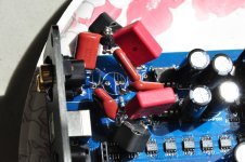
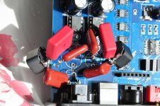
NOS Droop Filter pics
Here's some pics of my NOS Droop filter. Sorry for the "dramatic" lighting, I was using the morning sun coming in through the window. Should have added the flash.
I also meant to take pics before soldering them to the PCB, but forgot. I think it's harder to see all the connections when they are in "air sculpture" form. But hopefully someone will get some value out of these pics.
Note I have a capacitor in series with the RCA connectors for DC-blocking.
Attachments

My take on that filter with abraxalito's values for my 10K preamp.
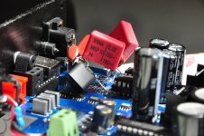
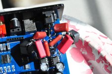
Gone quite far on messing the board, borken two tiny solder pads, first attempt I've made a short with one coil and these RCs barley fit (as caps) under the PCB. It's in and I'm scared to re-open the case... BTW, enough for me now on that gear but the AD844 to try. Will report my feelings about sound soon. Enjoying yours Matt?
Gone quite far on messing the board, borken two tiny solder pads, first attempt I've made a short with one coil and these RCs barley fit (as caps) under the PCB. It's in and I'm scared to re-open the case... BTW, enough for me now on that gear but the AD844 to try. Will report my feelings about sound soon. Enjoying yours Matt?
Attachments
Gone quite far on messing the board, borken two tiny solder pads, first attempt I've made a short with one coil and these RCs barley fit (as caps) under the PCB. It's in and I'm scared to re-open the case... BTW, enough for me now on that gear but the AD844 to try. Will report my feelings about sound soon. Enjoying yours Matt?
Nice work fitting the filters on the bottom of the board. When I added the transistors for biasing the opamps into classA, I gave up any chance of ever getting my board back in the case. Now the "naked" PCB just sits on my desk, upside down (which makes my DAC supply cap "load bearing", since it's one of the tallest).
Looks like you also pulled half your DAC chips. Did you find that to be an improvement?
Anyway, I'm absolutely enjoying mine. Enjoying it on multiple fronts, really: the sound coming out of it, learning a bit about how it all works, and making the actual modifications.
- Home
- Source & Line
- Digital Line Level
- TDA1387 x8 DAC: let's check its design, mod it -or not-, play music -or not! :(-