SMPS Bus pumping
SMPS Bus pumping
In this video I am showing the bus pumping when connecting the SMPS to the Class-D amplifier.
However, I found that the easiest solution to fix that problem is to add extra capacitance at the output of the SMPS.
In my video, I am using extra capacitance of 12500uF per rail, Using lower values of capacitance at the output will work, I just used the maximum value for my SMPS.
https://youtu.be/wrDNpEGmLKQ
Regards
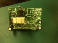
Welcome to the club of LiteAmp owners - ... hope that the results are worth to go through the pain of my unfriendly mechanical construction. 😀...showing a video of my setup, loading the amplifier 2 Ohms...
Many thanks for sharing your measurements, pictures and the video.
Welcome to the club of LiteAmp owners - ... hope that the results are worth to go through the pain of my unfriendly mechanical construction. 😀
Many thanks for sharing your measurements, pictures and the video.
In a few days, I will test the amplifier with some friends, to check the sonics.
I really thank you for bringing this amplifier to us, nice R&D, high stability, passed many critical tests.
I never liked the IRS2092 chip, because I never seen a stable (DIY version) like yours. so I never got convinced of building an amplifier using that chip.
However, I am running the amplifier at 420Khz.
Thanks
There is no way to comment on your smps as long as you do not disclose any details.
What kind of details you are looking for?
I am designing & developing SMPS for living, and i cant see a problem testing the amazing SYSTEM_D amplifier using my SMPS.
What kind of details you are looking for?
I am designing & developing SMPS for living, and i cant see a problem testing the amazing SYSTEM_D amplifier using my SMPS.
I would look for the usual details of interest: Schematics and building instructions of the transformer. Obiously you are not willing to share your smps designs. That is just not what I call "DIY-SMPS".
However in this application it will work to substitute 2SC5171 with a BD239C
and to substitute the 2SA1930 with a BD240C.
Hi Choco,
I tried using BD239C and BD240C in one of my gain boards and during step one of "getting it going" I have severe oscillation on the emitters of both devices with the 3k3 resistor tying them together. If I remove the resistor I get 11V on the NPN emitter and 10.6V on the PNP emitter with a +/-20V input. Any ideas?
SMPS Bus pumping
In this video I am showing the bus pumping when connecting the SMPS to the Class-D amplifier.
However, I found that the easiest solution to fix that problem is to add extra capacitance at the output of the SMPS.
In my video, I am using extra capacitance of 12500uF per rail, Using lower values of capacitance at the output will work, I just used the maximum value for my SMPS.
https://youtu.be/wrDNpEGmLKQ
Regards
It is good information for those that have not come across bus pumping before. Thanks.
If I remove the resistor I get 11V on the NPN emitter and 10.6V on the PNP emitter with a +/-20V input. Any ideas?
I guess it is -10.6V at the emitter of the PNP?
If so , then your description would point to heavy fluctuations of the +/-20V.
Do you measure similar fluctuations also at the +/-20V?
I guess it is -10.6V at the emitter of the PNP?
If so , then your description would point to heavy fluctuations of the +/-20V.
Do you measure similar fluctuations also at the +/-20V?
Yes, sorry, -10.6V at the emitter of the PNP. No fluctuations in the +/-20V, I am using a regulated dual bench supply. Behavior does not change if I increase the supply to +/-30V.
Hm, strange - can you describe the oscillations more detailed?No fluctuations in the +/-20V, I am using a regulated dual bench supply. Behavior does not change if I increase the supply to +/-30V.
Which frequency? Which magnitude? Any method of describing your observation is helpful. Verbal description or screenshots or a video showing your set up and measurement...
Hm, strange - can you describe the oscillations more detailed?
Which frequency? Which magnitude? Any method of describing your observation is helpful. Verbal description or screenshots or a video showing your set up and measurement...
Choco was kind enough to PM me with the offer of assistance in the background, but I believe hashing out this oscillation issue might be of help to others, so I am including some screen shots. With a 3k3 resistor tying the emitters together, I am seeing oscillation of around 10.8MHz. Without the 3k3 resistor I am seeing approx. +/-11Vdc on the emitters and the output is clean.
Power is provided by a dual bench supply with +/-20Vdc input voltage.
Thanks!
Attachments

Hi Ungie,
theoretically this oscilation should disappear when you place
R112 and R113 (==> Low HF load impedance in combination with C107 and C108, like a zobel).
Somehow my sample was more forgiving and did allow operation
without R112 & R113.
If you are afraid of causing defects to your OP amp in case the
oscillation would not disappear with R112 & R113, then you can
try it without risk first, simply by placing a series connection of 6R8+100nF from each emitter to GND.

Choco
theoretically this oscilation should disappear when you place
R112 and R113 (==> Low HF load impedance in combination with C107 and C108, like a zobel).
Somehow my sample was more forgiving and did allow operation
without R112 & R113.
If you are afraid of causing defects to your OP amp in case the
oscillation would not disappear with R112 & R113, then you can
try it without risk first, simply by placing a series connection of 6R8+100nF from each emitter to GND.
Choco
Hi Ungie,
theoretically this oscilation should disappear when you place
R112 and R113 (==> Low HF load impedance in combination with C107 and C108, like a zobel).
Somehow my sample was more forgiving and did allow operation
without R112 & R113.
If you are afraid of causing defects to your OP amp in case the
oscillation would not disappear with R112 & R113, then you can
try it without risk first, simply by placing a series connection of 6R8+100nF from each emitter to GND.
Choco
Thanks for the suggestion Choco, I will give that a try and report back.
Group buy?
Thanks for sharing this excellent little amplifier with us Choco
Is there any chance of another group buy for PCBs? Thought I'd ask before I order me some parts.
Thanks for sharing this excellent little amplifier with us Choco
Is there any chance of another group buy for PCBs? Thought I'd ask before I order me some parts.
...cannot talk for others, but from side I do not intend another group buy.
==> PM for you regarding few left over PCBs.
==> PM for you regarding few left over PCBs.
Unity gain
Hi,
A friend pointed me to this excellent project.
I have a little question. Obviously, lowering gain for this Amplifier helps reduce noise and THD. A gain of 5.6 is already very low for a Power amplifier. So we need extra stages etc.
As this is DIY, one wonders, is there any reason not to lower gain even more? If we lower gain to -1.1 noise should be another 5 times lower, as should be THD.
Making a small discrete circuit, that can run on the same rails as the Class D Amplifiers and delivers enough voltage into a few kOhm load is not difficult.
We could use something like the blameless amp from D. Self as the voltage gain stage deleting the final output pair.
Or for people who like tubes, why not tubes? This too can be made to have low THD, like the Aikido from John Broskie. So not a Moskido but a D-Lite Aikido.
Now what do we need to change on the Lite Amp BOM to make it unity gain, while reducing THD and Noise. I do not know much feedback theory and stuff so I am not sure where to start...
If we just make the input resistor 22K instead of 3.3K add an Aikido board and be done?
I'm pretty sure a Lite Amp + Aikido could become one of the most popular projects here.
Cheers
Lowering gain will bring massively underproportional improvements.
Besides the input noise of the OTA there are other noise sources, which are notfully canceled by the feedback. I.e. layout. I think for another big step of noise improvement you would need to go for fully differential signal handling, which is not supported by the IRS2092.
Regarding THD your goal seems to be a higher loop gain.
1. You do not automatically get higher loop gain by lowering the total gain.
2. Limitations of achievable loop gain are resulting from the output filter and higher order loop gain adjustment networks. These limitations will catch you independent from the target closed loop gain. I think with the chosen structure and output filter the LiteAmp already has a squeezed loop gain at the limit of reasonable engineering.
3. When you just change the input resistor, you will get also a reduced bandwidth of the input filter.
Last edited:
Enough to be dangerous, apparently. 😉 I routinely suggest Tim Green's series on op amp stability as an introduction to loop modeling. For noise there's an abundant amount of information around with particularly extensive design information from Analog and TI.I do not know much feedback theory and stuff so I am not sure where to start...
It seems you've some familiarity with noise gain but, as Choco's kindly pointed out, it's a mistake to assume all noise sources are input referred. Additionally you'll want to look at nested loop stability. The error you're making there is skipping over the parts of the IRS2092 datasheet and LiteAmp schematics indicating multiloop. It's a nontrivial topic and you'll likely have an easier time starting with class AB on a separate thread. But, to rephrase Choco's answer a little, outer loop gain is power stage limited. This makes it harder to stabilize the control device with increasing outer loop gain rather than easier; refer to the nCore patents and Bruno's discussion for a sense of the difficulty.
To put LiteAmp optimization in context, the LiteAmp, nCore, and Modulus-86/Parallel-86 are the three highest loop gain power amplifiers I'm aware of. They're all within a few dB of each other at the upper end of the audible range with the LiteAmp and Mod/Par unambiguously outperforming the nCore below 10 kHz. It's not difficult to meaningfully exceed these three at 20 kHz. But, unless engaging in very serious racket science, one has to accept output powers of a few hundred milliwatts to a couple watts to do so.
There's also the problem of delivering any additional loop gain at the power amp end of the speaker wire to the drivers, which is equally nontrivial.
Hi,
Hmmm, too bad.
Just looking at your FFT the noise floor seems uncorrelated and seems to correspond to the Datasheet values scaled by loop gain..
If it was related to switching etc., should we not see spurs or other correlated noise, rather than a flat thermal noise floor? Looking at it, I doubt I could do better than your layout anyway.
I am no EE (you can tell), why if I lower overall gain does loop gain not go up? I think for the audio band we can largely disregard the other loops.
I understand I change the corner of the input filter. If I calculate right it shifts from 122kHz to 80kHz. I think this is okay, or we can lower the cap to 680p to compensate.
So, the bottom line is, you do not think lowering gain further will help noise and lower THD. Too bad. Could we implement "AFEC" instead?
Augmented Feedback Error Correction (AFEC)
And what if we still want to use the Lite-Amp as a class d "power buffer", without gain, even if we do not lower THD & Noise by a factor of five?
Can the "change input resistor to 22k" (and adjust input filter capacitor or not) method be used? Or will it impact stability?
Sir S
Lowering gain will bring massively underproportional improvements. Besides the input noise of the OTA there are other noise sources, which are notfully canceled by the feedback. I.e. layout. I think for another big step of noise improvement you would need to go for fully differential signal handling, which is not supported by the IRS2092.
Hmmm, too bad.
Just looking at your FFT the noise floor seems uncorrelated and seems to correspond to the Datasheet values scaled by loop gain..
If it was related to switching etc., should we not see spurs or other correlated noise, rather than a flat thermal noise floor? Looking at it, I doubt I could do better than your layout anyway.
Regarding THD your goal seems to be a higher loop gain.
1. You do not automatically get higher loop gain by lowering the total gain.
2. Limitations of achievable loop gain are resulting from the output filter and higher order loop gain adjustment networks. These limitations will catch you independent from the target closed loop gain. I think with the chosen structure and output filter the LiteAmp already has a squeezed loop gain at the limit of reasonable engineering.
3. When you just change the input resistor, you will get also a reduced bandwidth of the input filter.
I am no EE (you can tell), why if I lower overall gain does loop gain not go up? I think for the audio band we can largely disregard the other loops.
I understand I change the corner of the input filter. If I calculate right it shifts from 122kHz to 80kHz. I think this is okay, or we can lower the cap to 680p to compensate.
So, the bottom line is, you do not think lowering gain further will help noise and lower THD. Too bad. Could we implement "AFEC" instead?
Augmented Feedback Error Correction (AFEC)
And what if we still want to use the Lite-Amp as a class d "power buffer", without gain, even if we do not lower THD & Noise by a factor of five?
Can the "change input resistor to 22k" (and adjust input filter capacitor or not) method be used? Or will it impact stability?
Sir S
- Home
- Amplifiers
- Class D
- SystemD LiteAmp