Terry please measure the resistance between the output (at the tab connector) and at the ground connector.
Hi Andrew,
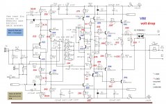
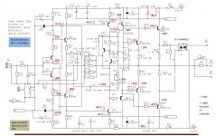
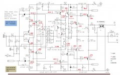
It is 555ohms. I will try to sit down today and create a couple schematics. One with VBE for each transistor and voltage drops on resistors and another with voltage to ground. Somehow I have to get to the bottom of this. Obviously, these boards can produce a working amp so I must have a bad or wrong part somewhere. I need to find it before I blow up any more parts.
Blessings, Terry
Do have all the parts now exept for the smd triac
What is the part number that you're missing?
Thanks
Do
OK, I sat down and measured everything. I marked up two schematics. One with VBE and resistor drops. The other has voltages compared to ground. I can see that the voltage at the base of the NPN outputs is low so I replaced Q12 again with no change. Hopefully one of these two schematics will help.
Thanks, Terry
Thanks, Terry
Attachments
What is the part number that you're missing?
Thanks
Do
This one from Mouser 512-FODM3012R2VNF098
Terry, on the LHS what is the output voltage? Are these readings with or without the offset dialed out?
I'm sorry, I don't know what LHS is. These measurements were taken with the offset as low as it will go. The pot is full counter clockwise.
Left hand side
Can you measure the junction of R1 and C1 and see that you can adjust it from +10V to -10 V.
Can you measure the junction of R1 and C1 and see that you can adjust it from +10V to -10 V.
Hi Andrew,
There was one thing that I noticed and forgot to note on the schematic is that the voltage at the junction of R1 and R3 is -10.32V. If I adjust R3, the voltage will move toward zero but the offset becomes more negative. I'm not sure if that matters but it is something that didn't seem right to me.
Thanks, Terry
Attachments
Last edited:
This does not seem right. If you measure at the junction of R3 and R1 you should get smooth adjustment from -10 V all the way to + 10 V. The amplifier output offset adjustment range should be about +-0.5 V IIRC. Can you recheck the voltage at the junction of R1and R3 and that you get the full -10 to +10 adjustment range?
Hi Andrew,
OK I just checked. If I adjust R3 until I read +10.3 at R1, the offset is -1.372V. With it adjusted to 0V at R1 the offset is -.822V. With R3 adjusted to -10.31 the offset is -.244v.
OK I just checked. If I adjust R3 until I read +10.3 at R1, the offset is -1.372V. With it adjusted to 0V at R1 the offset is -.822V. With R3 adjusted to -10.31 the offset is -.244v.
Ye, R1 is 10k. I just removed C1 and no change.
It stands to reason that there is offset. The bases of the N outputs are only .323V and the P channels are -8.22V. The question is why?
It stands to reason that there is offset. The bases of the N outputs are only .323V and the P channels are -8.22V. The question is why?
Last edited:
It looks to me like there is a problem in the front end that's causing an offset. If I look at all the other voltages, they seem to be in the correct ballpark.
It could either be a wrong value (check all the 15 Ohm resistors and locations) or a solder flash (i.e. bridge or short) somewhere. The symptoms you are seeing could also be because of very high gain - eg if R11 was shorted or very low value. One thing you could do is inject an input signal and check that the gain is about 37x and not much higher (remember to keep J2 shorted otherwise your gain will be 19).
I have to start work now, but will check back in a few hours again. Hopefully we can make some progress.
I think VBE matching for Q9-Q10 and Q8-Q11 is importance. I sim several alternative for Q9,Q10, Q8, and Q11 and only with BC550C/BC560C I can set the DC offset.
This one from Mouser 512-FODM3012R2VNF098
No luck on that one, Fab gave me what he had left when I started building the amp. Sorry!
Do
No luck on that one, Fab gave me what he had left when I started building the amp. Sorry!
Do
Then I've to wait till April
- Home
- Amplifiers
- Solid State
- SX-Amp and NX-Amp