Hi Keantoken,
The phase lead cap (shunt cap across feedback resistor RF) is a zero in the global loop of the amplifier, so it addresses phase loss which may be due to poles anywhere in the amplifier.
"Most people seem to assume that phase lead is the phase lead cap's only function but it is good to check whether something is doing what you think it is doing. If you do that, especially with slow input transistors you may find the feedback network is not having the expected frequency response. "
Agree. You do need to consider the effect of the input capacitance of amplifier when setting C_LEAD. With C_LEAD, the gain of your amplifier transitions from 1+RF/RG to 1 + C_IN/C_LEAD, where C_IN is the amplifier input capacitance at the minus terminal.
"Thus you often end up needing a phase lead cap NOT because you need extra phase for the VAS or output, but because nothing is charging the LTP diff capacitance and that is causing a pole and associated mayhem." This implies that the pole due to the feedback network and the input capacitance of the amplifier is the most critical. I disagree.
Let's take a look. This pole is an R on C pole, so let's look at both:
Resistance: The Thevenin resistance of the feedback network at the minus terminal of the amp is RF||RG = ~RG since RG = RF / (Close loop gain - 1). For example, for the Honey Badger this is 820 ohms.
Capacitance: The capacitance of the undegenerated (*) LTP is 2*C_PI + C_MU. For the MPSA18 (Honeybadger) this works out to be 2*5.5p+2p = 13p based on datasheet values. Give it 2pF more for board parasitic if laid out properly, so 15pF.
This R and C combination gives a pole at ~13MHz. The loop gain unity gain frequency (UGF) for an audio amplifier is usually between 0.5 and 1 MHz for the good ones, so a pole at 13MHz is going to give < 6 degrees of phase loss, so not that critical. Even if the capacitance was 30pF (say I grossly miscalculated), the pole would be at 6.5MHz (~10x above the UGF of most amps).
Bottomline here is: C_LEAD will help you where you need it. Do you need to consider the input capacitance of the amp when calculating C_LEAD? Absolutely. Is RF||RG on C_IN the most critical pole? No, it is just as bad as the rest.
"The same applies to source impedance at the input side. But the phase lead cap is magnified by Miller effect, so to have the equivalent effect on the input side your source capacitance (provided by the input shunt cap) needs to match the effective miller capacitance." I think I agree, but I need to think about this one more.
I understand the lead cap will see gain across it, and hence it is Miller multiplied when looking at it from the minus terminal of the amplifier. RF sees the same effect, but it is shunted by RG so it does not matter on RF... hmm, ok, until I can think of a counter argument, I will say I agree.
"Note that opamps can use custom input transistors or Darlingtons whereas most amp designs just have a simple LTP with general purpose transistors which will have much much lower input impedance than an opamp input. This is a major factor that leads to many of the differences between discrete amps, power amps, and opamp designs."
I disagree on this one. The number of transistors out there is huge, just look at ON's catalog, so there are plenty of choices for discrete design. The major differences between discrete amps, power amps, and opamp designs are:
- COST: In an IC a transistor is free. You can pack so many transistors with no impact on cost that you don't think about it when adding one. In a discrete design, any component you add will cost you money.
- MATCHING: In an IC you can match resistors and transistors easily (and cost effectively). In a discrete design, getting a matched resistor network will cost you many $. And, if you want to get a good transistor match pair, it will not only cost $, but your selection now shrinks enormously.
- PARASITICS: In an IC, components are so close to each other that the parasitic capacitance to ground or between components is really small, small fractions of pF. In a board, with proper layout, you are in 1-2pF for nodes you pay attention to, and many more for those that you don't.
- RELIABILITY: In a discrete design, any extra component you add you are increasing the likelihood of it failing. Failures will range from poor soldering to a bad component batch to who knows. You can equate reliability to cost, since servicing a device is not free. Hence in discrete, you are compelled to keep component count as low as you can get away with. In ICs this is not the case. Reliability is not impacted much by component count, it is usually due to packaging issues, fab defects that affect all components, bonding issues, etc.
As a result, in discrete design you are compelled to do simpler topologies with than in ICs. Specially due to cost, nobody likes to overpay (actually, I should not say nobody).
Finally "Should I work at AD? Do I stand a chance at getting in?" PM me if you are interested. I don't work at ADI anymore, but I still have plenty of friends there.
Thanks for the comments Keantoken.
Best, Sandro
(*) I did the calculation using the undegenerated diff-pair even though all decent amplifiers have a degenerated diff-pair. Degeneration adds a zero to the CPI component input capacitance of the LTP, i.e. after the frequency 1/(2pi*RE*CPI), the CPI component does not look capacitive anymore, it looks resistive. For RE = 100, for an MPSA CPI of 5.5pF, this is about ~290MHz, so we can ignore the effect of the resistor.
Last edited:
Okay, all valid points, maybe I was a bit overzealous on this issue. I agree that the phase lead cap doesn't single out any specific phase shift. However it can only compensate one pole. And that will probably be the next or 2nd pole after Cdom. So it isn't strictly accurate that it will address any phase shift.
If you are designing for high BW, then your phase lead cap needs to be as low as possible as it sets your BW limit. And that means the diff capacitance may contribute substantially to the phase you are mitigating. For a high OLG design, you need to reduce OLG at unity as far as possible and that means you want the maximum CLG hence it becomes a high BW design and the phase lead cap must be small.
Also your capacitance is wrong. Think about what I'm saying. Differential capacitance isn't only Cob. Cje is usually many times larger than Cob and it astounds me how many people don't consider this. If your LTP has 5mA per transistor that is a Rm of 0.027/0.005=5.4ohms. If the Ft is 100MHz then Cje is the capacitance where Ib=Ic at that frequency. So 1/(2pi*5.4ohm*100MHz)=295pF (minus Cob which contributes slightly to Ft). Both emitters in series makes 148pF. Some people use slower transistors like the MPSA42 so this can become a huge issue.
So your diff capacitance is 148pF. This means that if your source capacitance is 150pF then your amp will behave as if your LTP Gm has been halved, as the diff voltage reflected across the source capacitance subtracts from your expected differential voltage.
However we're not done. We can minimize this by choosing the transistor with highest Ft, but we also want high Beta otherwise source impedance will cut into THD figures (by the same mechanism, altering the effective LTP Gm). And it turns out that high-beta transistors usually have high Rb. The MPSA18, BC550 and family usually have on the order of 160-1k Rb. And this introduces a pole that is much less easily dealt with as it is a real pole in Gm and not just an effective one.
Degeneration does reduce these effects but I tend not to use it, go figure.
The pole caused by the differential capacitance is at the corner frequency of Cdiff and your source resistance. So if you have a 470ohm feedback shunt resistor, your pole will be at 1/(2pi*148pF*470)=2.3MHz. For the MPSA42 it would be 700KHz.
"If you are designing for high BW, then your phase lead cap needs to be as low as possible as it sets your BW limit. And that means the diff capacitance may contribute substantially to the phase you are mitigating. For a high OLG design, you need to reduce OLG at unity as far as possible and that means you want the maximum CLG hence it becomes a high BW design and the phase lead cap must be small."
Yes and no. Lets call the lead cap CF and CIN the input cap of the amplifier. If you dial the CF such that CF = CIN/(CLG - 1) then you get a perfect transition from resistor feedback network to a capacitive feedback network where both are set to give you the same CLG. We do this in fixed gain op-amp amplifiers.
"Also your capacitance is wrong."
You are right, I screwed up the CBE capacitance for the MPSA18. I used the capacitance in the spec table, which says it is 5.5pF for IC=0. Did not notice it until now.
For IC <> 0, you have to use FT as you did. I use a bit different nomenclature, but that makes no difference. Using C_BE = CPI, C_BC = CMU:
Ft = 1/(2pi*(CPI+CMU)) = ~1/(2pi*CPI) as you mentioned.
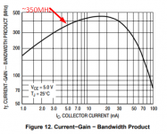
For the MPSA18, FT=350MHz, so in that case CPI= ~90pF and C_IN = CPI/2 = 45pF. (I screwed this up too since I said x2 and /2).
For FT=100MHz, I agree, CPI=~300pF and C_IN=~150pF.
For the Honey Badger which uses the MPSA18 and RG=820ohms, you get 4.3MHZ.
If you go with the KSA992 which has FT=100MHz and thus C_IN=150pF, and RG=420, you get 2.3MHz as you mention.
"So your diff capacitance is 148pF. This means that if your source capacitance is 150pF then your amp will behave as if your LTP Gm has been halved, as the diff voltage reflected across the source capacitance subtracts from your expected differential voltage."
This is true after Cshunt has taken over the resistance at the PLUS node of the amplifier. If RS=820ohms (Honey Badger) and Cshunt = 270pF (Honey Badger), then this won't happen until 124MHz. [The Rin of the overall Amp as seen from the input jack goes down much earlier, but the impedance as seen by the internal amp plus terminal goes down at 1/(2pi*RS*Cshunt).]
Therefore the effect you quote is not valid at frequencies of interest. What is true and will get you is the pole at RG with C_IN as discussed above.
The MPSA18, BC550 and family usually have on the order of 160-1k Rb
Where did you get this? It is not in the datasheet.
Best, Sandro
Yes and no. Lets call the lead cap CF and CIN the input cap of the amplifier. If you dial the CF such that CF = CIN/(CLG - 1) then you get a perfect transition from resistor feedback network to a capacitive feedback network where both are set to give you the same CLG. We do this in fixed gain op-amp amplifiers.
"Also your capacitance is wrong."
You are right, I screwed up the CBE capacitance for the MPSA18. I used the capacitance in the spec table, which says it is 5.5pF for IC=0. Did not notice it until now.
For IC <> 0, you have to use FT as you did. I use a bit different nomenclature, but that makes no difference. Using C_BE = CPI, C_BC = CMU:
Ft = 1/(2pi*(CPI+CMU)) = ~1/(2pi*CPI) as you mentioned.
For the MPSA18, FT=350MHz, so in that case CPI= ~90pF and C_IN = CPI/2 = 45pF. (I screwed this up too since I said x2 and /2).
For FT=100MHz, I agree, CPI=~300pF and C_IN=~150pF.
For the Honey Badger which uses the MPSA18 and RG=820ohms, you get 4.3MHZ.
If you go with the KSA992 which has FT=100MHz and thus C_IN=150pF, and RG=420, you get 2.3MHz as you mention.
"So your diff capacitance is 148pF. This means that if your source capacitance is 150pF then your amp will behave as if your LTP Gm has been halved, as the diff voltage reflected across the source capacitance subtracts from your expected differential voltage."
This is true after Cshunt has taken over the resistance at the PLUS node of the amplifier. If RS=820ohms (Honey Badger) and Cshunt = 270pF (Honey Badger), then this won't happen until 124MHz. [The Rin of the overall Amp as seen from the input jack goes down much earlier, but the impedance as seen by the internal amp plus terminal goes down at 1/(2pi*RS*Cshunt).]
Therefore the effect you quote is not valid at frequencies of interest. What is true and will get you is the pole at RG with C_IN as discussed above.
The MPSA18, BC550 and family usually have on the order of 160-1k Rb
Where did you get this? It is not in the datasheet.
Best, Sandro
Last edited:
So my figure of 100MHz was pessimistic for MPSA18 and BC550. Also my most recent work has been in designing discrete opamps, so maybe my off the cuff figures are not concerning for audio amps where the GBW is much lower.
Rb values change depending on manufacturer, but I have ballpark values from other people's measurements at 170R for the BC550C, 320R for the MPSA18 and 15R for the MPSA42.
The MPSA18 doesn't have Ft specified at 5mA so I will stop using it as an example.
For the BC550C, Ft is 340MHz at 5mA. Cje=87pF. So 170R+820R and 87pF/2=43pF gives a pole frequency in the open loop response of 3.7MHz.
At 5mA as in the example I gave, Ft for MPSA42 is 30MHz, not 100MHz (it changes with current, do NOT use the table value). Rb is 15 ohms, so
Cje = 1/(2pi*5.4*30MHz) = 983pF
Fc = 1/(2pi*983pF/2*(15R+820R)) = 388KHz
Wow, not very good if the MPSA42 had been used in the Honey Badger.
This is easiest to think of as a pole in the LTP Gm, but maybe that is just me and is confusing everyone else.
You are making a mistake in treating diff capacitance the same as input capacitance. Diff capacitance generates current according to differential voltage, not feedback node voltage. Thus it does not behave like a capacitive divider in the way you described. Instead the contribution of Cdiff to output voltage is Vout=Vdiff*(Cdiff/Clead), ignoring the contribution of the gain resistors and input voltage.
The 270pF dominates input side source impedance above
Fc = 1/(2pi*270pF*820R) = 719KHz
Rb values change depending on manufacturer, but I have ballpark values from other people's measurements at 170R for the BC550C, 320R for the MPSA18 and 15R for the MPSA42.
The MPSA18 doesn't have Ft specified at 5mA so I will stop using it as an example.
For the BC550C, Ft is 340MHz at 5mA. Cje=87pF. So 170R+820R and 87pF/2=43pF gives a pole frequency in the open loop response of 3.7MHz.
At 5mA as in the example I gave, Ft for MPSA42 is 30MHz, not 100MHz (it changes with current, do NOT use the table value). Rb is 15 ohms, so
Cje = 1/(2pi*5.4*30MHz) = 983pF
Fc = 1/(2pi*983pF/2*(15R+820R)) = 388KHz
Wow, not very good if the MPSA42 had been used in the Honey Badger.
This is easiest to think of as a pole in the LTP Gm, but maybe that is just me and is confusing everyone else.
Yes and no. Lets call the lead cap CF and CIN the input cap of the amplifier. If you dial the CF such that CF = CIN/(CLG - 1) then you get a perfect transition from resistor feedback network to a capacitive feedback network where both are set to give you the same CLG. We do this in fixed gain op-amp amplifiers.
You are making a mistake in treating diff capacitance the same as input capacitance. Diff capacitance generates current according to differential voltage, not feedback node voltage. Thus it does not behave like a capacitive divider in the way you described. Instead the contribution of Cdiff to output voltage is Vout=Vdiff*(Cdiff/Clead), ignoring the contribution of the gain resistors and input voltage.
This is true after Cshunt has taken over the resistance at the PLUS node of the amplifier. If RS=820ohms (Honey Badger) and Cshunt = 270pF (Honey Badger), then this won't happen until 124MHz. [The Rin of the overall Amp as seen from the input jack goes down much earlier, but the impedance as seen by the internal amp plus terminal goes down at 1/(2pi*RS*Cshunt).]
The 270pF dominates input side source impedance above
Fc = 1/(2pi*270pF*820R) = 719KHz
Last edited:
Sorry, I just realized the low Ft of the MPSA42 is due to quasi-saturation in the measurement, so I think the actual Ft at 5mA is around 100MHz. So
Cje = 1/(2pi*5.4*1000MHz) = 295pF
Fc = 1/(2pi*295pF/2*(15R+820R)) = 1.29MHz
Cje = 1/(2pi*5.4*1000MHz) = 295pF
Fc = 1/(2pi*295pF/2*(15R+820R)) = 1.29MHz
I have not done any rb measurements on discretes, so I take your values on faith.Rb values change depending on manufacturer, but I have ballpark values from other people's measurements at 170R for the BC550C, 320R for the MPSA18 and 15R for the MPSA42.
Yes it does. See attached screenshot.The MPSA18 doesn't have Ft specified at 5mA so I will stop using it as an example.
Let me do an experiment and I'll get back to you.You are making a mistake in treating diff capacitance the same as input capacitance. Diff capacitance generates current according to differential voltage, not feedback node voltage. Thus it does not behave like a capacitive divider in the way you described. Instead the contribution of Cdiff to output voltage is Vout=Vdiff*(Cdiff/Clead), ignoring the contribution of the gain resistors and input voltage.
Man, today I am really off doing mental math... brain is tired. You are right, Cshunt will dominate at 720kHz. That is a problem since it is right where it hurts. For my amp, RS=75 and CS=680p, so at least I pushed out the issue to 3.1MHz.The 270pF dominates input side source impedance above. Fc=1/(2pi*270pF*820R) = 719KHz
Anyway, thanks for the discussion. I'll get back to you on the CDiff stuff.
Best, Sandro
Attachments
BTW, are you designing discrete op-amps for work, for a specific project/purpose, or just for fun?
The reason I ask is because if it is for fun/learning purposes anything is fair game.
If for a specific project, I assume you are trying to achieve something you cannot with an off the shelf one like very high voltage. Is this the case?
Else, I would not bother, discrete op-amps do not stand a chance against integrated ones. I know I am mega biased, but it is true.
If for a specific project, I assume you are trying to achieve something you cannot with an off the shelf one like very high voltage. Is this the case?
Else, I would not bother, discrete op-amps do not stand a chance against integrated ones. I know I am mega biased, but it is true.
Sandro, this series is great and the audio has materially improved. You've done good work and it's been a good refresher and tips/tricks for LTSpice as well.
Well, for low noise you can drive the opamp with your own low noise input stage, and avoid designing the rest of the circuit with discretes.
Actually, 1nV/rtHz is not a challenge for IC op-amps. The AD797 is 0.9 nV/√Hz and that op-amps as great as it is, is getting old.
Hi Phoenix, I missed the FET input piece. Yes, that is discrete op-amp land. 1nV/rtHz is not hard for BJT, but FET is another story. My favorite FET op-amp, the OPA140 is 5nV/rtHz.
Sorry about that.
Best, Sandro
Sorry about that.
Best, Sandro

Hello Sandro ,
How much of an impact on the total distortion of an amplifier would a multi-tanh input stage have of say a Thompson topolog, and is it to your knowledge ever used in audio opamps. I know Douglas Self in "Audio Amplifer Design Handbook 5th edition" makes mention of Cascomp page 88 figure 4.11(c) as an approach to improve input linearity but was not further developed . Is this a worth while approach for Audio Power amplifiers and if not where is it used , does it degrade the noise peformance. I notice that the audio opamp benchmark for noise and distortion is the AD797 and this uses undegenerated input transistors with no special additional circuit tricks to improve linearity ( I am referring to the input transistor circuit only).
How much of an impact on the total distortion of an amplifier would a multi-tanh input stage have of say a Thompson topolog, and is it to your knowledge ever used in audio opamps. I know Douglas Self in "Audio Amplifer Design Handbook 5th edition" makes mention of Cascomp page 88 figure 4.11(c) as an approach to improve input linearity but was not further developed . Is this a worth while approach for Audio Power amplifiers and if not where is it used , does it degrade the noise peformance. I notice that the audio opamp benchmark for noise and distortion is the AD797 and this uses undegenerated input transistors with no special additional circuit tricks to improve linearity ( I am referring to the input transistor circuit only).
Last edited:
Hi Phonenix, I have never seen a multi-tanh used in an audio-power-amp. But it has been used in op-amps.
How much of an impact on the total distortion of an amplifier would a multi-tanh input stage have of say a Thompson topology,
Depends on your starting point. If you go from say an undegenerated input stage to a doublet, you get more linear range in the input stage and less distortion. If you go from a heavily degenerated input stage to a doublet, your THD performance will go down, but your noise will improve.
and is it to your knowledge ever used in audio opamps.
Yes, several op-amps from ADI use a multi-tanh input.
Is this a worth while approach for Audio Power amplifiers and if not where is it used , does it degrade the noise peformance.
I would not use it in an Audio Power Amp. It is more suited for medium to high speed, low noise op-amps. It degrades noise performance when compared to a simple undegenerated diff-pair.
I am going to cover this when I get to input stages, but let me give you a preview on why they are not suitable:
- Say we have a 150W_RMS Power Amp, then Vout_peak = ~50Vp
- Also, say Loop Gain has a cross over frequency (UGF) of 500KHz, such the loop gain is 10 at 50kHz, and 25 at 20KHz.
- Finally, say the closed loop gain of the amplifier is 35 (input sensitivity of 1VRMS), then at 20KHz, the Open loop gain = 25x35 = 875.
Now, when the output is swing 50Vp at the output, the input stage will see 50V/875 = ~60mVp across it. A multi-tanh input stage does not have 60mVp linear range, so it will distort at full power 20KHz.
BUT, say you are in op-amp land and your swing is 5Vp, then, if everything else stays the same for easy comparison, the required linear range at 20KHz is 6mVp which you can achieve with a mult-tanh.
I know Douglas Self in "Audio Amplifer Design Handbook 5th edition" makes mention of Cascomp page 88 figure 4.11(c) as an approach to improve input linearity but was not further developed
I don't know why he did not develop it further. A cascomp is a good circuit.
I notice that the audio opamp benchmark for noise and distortion is the AD797 and this uses undegenerated input transistors with no special additional circuit tricks to improve linearity ( I am referring to the input transistor circuit only).
This is true. The AD797 aims to achieve low noise. Any trick you do, including multi-tanh, will degrade your noise vs. supply current figure of merit.
So how does the AD797 achieve good distortion at 20KHz with such basic input stage? Speed!
The GBW of the AD797 is 110 MHz, so at a closed loop gain of 1, the 20KHz open loop gain is 5500. Therefore, with a 5Vp signal at the output, the input stage sees 0.9mVp which still within the linear range of a simple diff-pair.
Bottom line: For audio amps you need to degenerate the input stage, this is your best option. To keep low noise use a high tail current in the diff pair to keep the degen. resistors small.
To improve THD due to the input stage, focus on reducing VBE distortion and IB distortion of the input devices. How? Stay tuned.
I hope this make sense and that I did not screw up any of my numbers 🙂.
Best, Sandro
Last edited:
- Home
- Amplifiers
- Solid State
- SW-VFA-01: Audio power amplifier video series