Hi Sandro,
excellent initiative, I am sure this will be helpful for many, I quickly checked through all 5 videos given in the first post, the video looks good, but let me cut to the chase, the audio quality has a bit too much room reverberation which is a sign the microphone is, for the given acoustics in your recording milieu, too far away, it would be much better if you have the microphone mounted on a boom arm and not more than about a foot away from your mouth, to get the idea how much better it can get check out the following video (which uses the same Samson Meteor microphone as you), go directly to 11:27 and compare that to other parts of the video when the microphone is standing on the desk (although his room seems to be better damped than yours so desk mounted still sounds better in his case).
YouTube - Samson Meteor Mic review (w/BONUS BLUE YETI sound comparison)
btw, I like the tinted background better than pure white, it is saving the eyes, it's actually not so much about taste but rather about eye health, LCD screens uses white LED background light which all have strong peak in the upper blue spectrum and is not good for the retina.
Cheers Michael
Thanks Michael! While I would love to get a boom arm, the chances of that happening are quite low. I do the recordings in my home office (not great acoustics) which I share with my wife. If she sees the boom arm, she will throw it away (she is into room aesthetics). What I will try to do is position the mic as best as I can to get it closer to me.
Quick question: I agree the audio on the first 2 videos was quite poor, but is the audio on the sub-subsequent videos better? More important, is it acceptable?
Thanks!
Actually a white LED is a Blue LED with a special phosphor covering it.
Thanks Sandrohv for the effort you put into the videos. I look forward to learning a lot from your efforts. I only wish that there was a Python interface to the LTSpice simulator. Keep up the GREAT work. Thanks
Thanks Kris!
Hi all, I got a great PM from Rick Savas, and I wanted to share it with everyone:
Hi Sandro,
I have your sim environment running. Couple of observations, it might because of my lack of ltspice knowledge, so will ask for clarification.
1) I see you have ".include DIYAamp.txt" but you did not provide this file. I made a dummy file using that name to get the sim to run. But wonder what is in the file, what it is used for?
2) When I run the ".op" sim, I went to the amp schematic, I usually place the cursor over a net and LMB click on the net to display the important voltages for display that I want to observe. When I select on the right side of R22, I get the supply V displayed properly, but when I try to display the V for the left side of R22 I get "???". So it seems it will only display nets connected directly to the symbol in the hierarchy. I am wondering if you know why that is and if there is a means to correct this behavior?
Thank you
Rick
1) Sorry for not including the file, my mistake. This is Oz's models file for the Honeybadger amplifier. I am attaching now. I grabbed it from the HoneyBadger thread as well as the schematic... so it is original 🙂.
2) I just tried it and I did not get that behavior. See the attached image. I can click any node on the the HB amp and get the voltages. These are the steps I did:
- Run simulation from HoneyBadgerTestBench.asc
- After the simulation was done, double clicked on the amp symbol to open the HB schematic
- Poked voltages in the HB schematic
See if that works.
Enjoy!
- Sandro
Attachments
Hi Sandro,
I watched the first two video’s, excellent, your ltspice test bench methodology is what I need to better use the simulator. I need to spend some time learning to use it to get more familiar with it.
What is the end goal? Is it making a working amplifier in an enclosure? If so, relay your thoughts for us following along on your journey.
Cheers
Rick
Hi Rick, that is a very good question...
Main goal: Teach everything I know and learn along the way on Audio Amplifier Design, leveraging what I know from 11 years of op-amp design.
Sub-goal: Design a few amps as we go through this. This will include an ultimate-amp (SW-VFA-01), a differential out amp (SW-VFA-02), a simplified amp (SW-VFA-03), etc. I'll refine the order as I go along.
Originally, I was thinking of jumping into designing an amp and showing it at various levels of completion, but then I realized this was not helpful for the many who are unseasoned at amp design.
Then I realized there is no video series on amp design, so why not create one, starting from scratch. Bob's and Doug's books are great, but they don't give you the hands on part, i.e. there is a value add on watching someone do the LTSpice sims and see what is going on. Also, watching someone designing an amp step by step shows you what is going through their heads and what trade-offs are being made.
Finally, for me, it gives me the opportunity to improve my communication skills and have some fun making videos. Also forces me to not get too far away from circuit design given I no longer design ICs.
I hope people get something out of this and are finding the videos useful (so far the response has been positive). I know we have not designed much yet since I am still running through the fundamentals, but I want to get as much groundwork covered as possible before designing the amp itself.
Best, Sandro
Last edited:
@sandrhohv,
yes I noticed that the first two videos had worse audio quality than the following ones which did sound better due to microphone upgrade, but I still think your high quality 1080p video deserves to have an audio quality matching the video, the distance to the microphone is crucial no matter if it's a cardioid type that helps a bit in picking up less of the surrounding noise, I really do encourage you working on the microphone placement and recording, after all we are on an audio forum so some of us have pickier ears so keep up the good work! 🙂
yes I noticed that the first two videos had worse audio quality than the following ones which did sound better due to microphone upgrade, but I still think your high quality 1080p video deserves to have an audio quality matching the video, the distance to the microphone is crucial no matter if it's a cardioid type that helps a bit in picking up less of the surrounding noise, I really do encourage you working on the microphone placement and recording, after all we are on an audio forum so some of us have pickier ears so keep up the good work! 🙂
This is probably not the correct explanation.Hi Damir, when you are looking at schematics and plots all day day on a screen, looking at a white background will tire your eyes. White paper is fine because unlike a screen, paper does not produce light, it simply reflects it and is less tiring on your eyes.
As the resident monitor snob, I would say that the main causes for monitor fatigue would have to be:
* excessive brightness (or far too little, which is much rarer)
* screen flicker, especially if the user is sensitive to it (like yours truly) and/or if there are flickery ambient light sources around
* to a lesser degree, color temperature, especially if >7000 K - blue further exacerbates flickering
* non-ideal positioning / sitting posture
* optimistically small font sizes
* undiagnosed presbyopia, especially in dim environments
Inexpensive monitors not uncommonly combine all of the first three right out of the box (possibly four if the stand isn't much to write home about), with backlight PWM running at a typical 200 Hz (I prefer about 600-700 and possibly higher) and inexpensive white LEDs on the bluish side of 6500 K. I must also have installed backlight PWM adjustment tools on dozens of older notebooks with Intel graphics, not to mention the customary calibration for something resembling half-decent colors (TN panels often have a major case of the blues). The switch to LED backlights from around 2010 onwards really brought out the issue of PWM flicker - something used before but previously covered up by the slower phosphors of CCFLs. It is a very common issue through about 2012 when the problem slowly started to be recognized as such.
CAD software traditionally uses white on black because in the olden days, you could never get enough resolution for this application and CRT monitors and graphics cards were really struggling to provide half-decent refresh rates. Large white areas at 70 Hz, 60 Hz or even 87 Hz interlaced (anyone remember 8514/A modes?) are pure hell on the eyes, while inverse display makes things a good deal more acceptable.
Due to my flicker sensitivity as a result of nystagmus (jittery eyes - something very common e.g. in those (once) afflicted with strabismus), I had never been entirely happy with CRTs, even at 85 Hz or 100 Hz. My first LCD monitor was nothing short of a godsend. Where my eyes used to resemble those of a rabbit after little more than 2-3 hours on the PC, 8+ suddenly wasn't a major problem.
My recommendations for minimum fatigue:
* Pick a monitor that uses either a very high PWM frequency or no PWM at all in the brightness range of interest. Some TVs in particular will also generate artificial flickering for better motion, turn this off if present for obvious reasons.
* Pick a display panel technology that gives you enough latitude for color adjustments to achieve a slightly warm color temperature (maybe 5800-6000 K, I wouldn't go much below or else photos won't look to great; and yes, what's called "warm" is a lower color temperature than what's called "cool", go figure). This is pretty much everything other than TN. If you are stuck with TN (I have seen some rather decent TN-Film panels from AUO, typically used by Taiwanese brands), pick a model with a warmish native color temperature.
* Make sure you have enough adjustments in the monitor stand, or at least a VESA mount so that a separate monitor arm can be used. Observe general ergonomic guidelines for PC workplaces.
* Adjust monitor brightness so that white isn't blindingly bright but rather blends in. If ambient light is not constant, automatic brightness functions on the monitor may be helpful.
* Make sure that commonly-used UI elements are at a comfortably large font size.
* Have a decent amount of (non-flickery) ambient light at all times. If you need a backlit keyboard it's probably too dark. However, don't overdo it either to avoid messing with your sleep cycle too much. It's probably a good idea to stick with 3000ish K in evenings / nighttime for the same reason (it is blue light that sets our internal clock).
* Those of you well in your 40s and beyond (so probably the majority around here) may want to get your eyesight checked. If minimum focus is beyond 0.5 m or even 1 m, some workplace glasses for moderate distances may be very well appreciated.
If you don't see flicker, you could still look into making some sort of photosensor to be used with an oscilloscope. This might traditionally be a photodiode with a transimpedance amplifier but more improvised solutions e.g. using LEDs or glass case diodes are certainly possible as well.
Last edited:
Hi all, I got a great PM from Rick Savas, and I wanted to share it with everyone:
Hi Sandro,
2) When I run the ".op" sim, I went to the amp schematic, I usually place the cursor over a net and LMB click on the net to display the important voltages for display that I want to observe. When I select on the right side of R22, I get the supply V displayed properly, but when I try to display the V for the left side of R22 I get "???". So it seems it will only display nets connected directly to the symbol in the hierarchy. I am wondering if you know why that is and if there is a means to correct this behavior?
Thank you
Rick
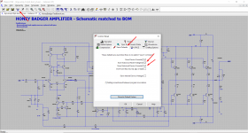
Hi Rick, I think I know what is going on. You need to tell LTSpice to store the voltages and currents in the sub-circuits. It is in the "Save Defaults" on the LTSpice control panel. See attached Screen shot.
I am not sure what the default is, but this should fix the problem.
Best, Sandro
Attachments
You got it Sandro,
I am an ltspice amateur, it shows 🙂 I was wonder why the log was so short of the usual long list of data 🙂
Funny how the two versions behave differently, adds to the confusion 🙂
I am going to have to beat your fantastically free ltspice lessons (eLearning) into my old brain 🙂 practice makes perfect ...
A bit off topic, somewhat curious, so have to ask, are you an EE that does or does not layout your own pcbs? Kind of a setup ? as to the direction of physical design aspect of these new designs.
I never laid out a chip before, did packaging/pin-out for an LSI ASIC once, did you do layout of your chip designs? If you think this is too off topic, you can reply to me in the PM or ignore me 🙂
On the monitor back ground colour subject, my 2 cents, I could never see myself doing any layout without a black background, it would fry my eyes & brain in short order otherwise. Video display systems measure contrast ratio as being very important, we/I want black black , lights off even, mushroom work ... 🙂
Is there a way to control the default colours ltspice uses for the plots? I know how to change them, but it is a PITA everytime to sub that dark blue default.
Cheers Rick
Last edited:
Hi Rick,
Here are some interesting facts about me...
1. Regarding LTSpice, I actually learned to use the program in December last year. Before I used the Cadence Design Suite which is more for IC design. So... I am learning too 🙂.
2. I have never laid out a PCB, so you can say I am an EE that does not lay out his PCBs. At ADI we have a team that exclusively lays out PCBs so all designs went through them. Basically, I gave them a schematic, placement guidelines, and then worked with them on the iterations till we got it right. I believe they used Alegro.
3. For IC layout, I did a little bit but never a full chip (mainly cells). Mostly due to time. There are layout engineers whose main job is to layout ICs. These guys are fast. Easily 10x faster than what I could do. So it was faster for me to tell them what to and have go at it.
4. And here is the natural follow up question. I am so so at building things, but eager to learn. So I am going to need help when the time comes to build these amps. I have been looking at the builds people make in this forum and some guys have some solid building skills.
Glad the setting worked out on your LTSpice.
Best, Sandro
Cool, thanks for letting me in on your experiences. That is correct Cadence Concept or OrCad Capture, for pcb schematic entry and I use the old OrCad Layout for simple boards, like these ones but Layout is obsolete now replaced with Allegro with its sub-sets of functionality/product names.
I used Mentor BoardStation too, now dating myself, I go way back to Cadnetix days, but that morf'd into VeriBest now Mentor Expedition IP 🙂
Got a free trip to Mentor HQ for training, so got to visit/tour your area in the mid 90's.
I guess the logical choice for you, if you want to fab your designs, might be to use KiCad, but I have never taken the time to learn that one, imo it is just a distraction, taking a different car and route to get to the same place 🙂
Take care Rick
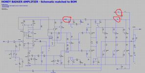
Hi all, in a couple of other threads I have been asked to share my version of the Honey Badger amplifier, and here it is (zip file). The circuit is v2.4 of the Honey Badger, with the following mods:
- All supply sources and input sources have been removed and replaced with pins
- A symbol had been added.
The zip file contains:
- Honey Badger schematic (.asc)
- Honey Badger symbol (.asy)
- Honey Badger test bench as shown in video 1.2
- Ozztripers models for this amplifier: DIYAamp.txt
Let me know if you have questions.
Best, Sandro
Attachments
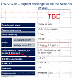
Hello Sandrohv.
>>THD: 0.001% worst case, 20KHz, max output power
A question you included a spec on THD shown above what is the ohm load, may I propose 2 ohm as good goal if thats possible.
Regards
A
>>THD: 0.001% worst case, 20KHz, max output power
A question you included a spec on THD shown above what is the ohm load, may I propose 2 ohm as good goal if thats possible.
Regards
A
I believe I said 8 ohms. See picture.
I will try with 2 ohms too, but remember that for 2 ohms output swing will go down if we want to keep output power constant. 150W into 8 ohms is 34.6VRMS and 150W into 2 ohms is 17.3VRMS.
Now if you are asking for full swing at 2 ohms, that would be 34.6V^2/2ohms = 600W. My amp won't be able to withstand that without blowing up the output devices. So not in scope 🙂.
EDIT: I just saw where you got it from, post #1. Fixed it just now to say 8ohms. Thanks!
Best, Sandro
Attachments
Last edited:
My mistake I did not read the spec completely. I think 17.3VRMS into 2 ohms would be a good test to achieve 0.001% THD 20Khz also.
4.1. Audio Amplifier Design Fundamentals: Two Stage voltage feedback amplifiers
Hi all, just to let you know that I just uploaded the next video of the series:
4.1. Audio Amplifier Design Fundamentals: Two Stage voltage feedback amplifiers
The video is a recap of the two stage voltage feedback amplifier. It also introduces the minor loop that has been talked about in many compensation threads.
Link to video: 4.1. Audio Amplifier Design Fundamentals: Two Stage voltage feedback amplifiers
Couple of things:
- Tried to shrink the length to 10 min, I get the feeling that my previous videos are too long
- Tried to improve the audio by getting the microphone closer, hopefully it worked
Enjoy,
Sandro (SW Audio)
Last edited:
Hi Sandro, I was fine with the length of the first few, actually found the latest ones too end abruptly, as if you were on some sort of time limit. No sense making them too short and missing details or allow for more elaborate descriptions, explanations. If they are too long, press pause, take a break and get back to it when you have more time. Just go for it, do not bother looking at the clock or keeping time.
Some of this stuff is new or really old to us/me at least 🙂 I have not used this math since college in the 70's, so the more detail the better imo. Have to remember what "s" stands for, "2pi*f", iirc 🙂
I was lying in bed watching it last night, the cell phone is not the best to use, due to its small screen but you came across very well, way better than my old fart prof's. Now I am the old fart. Great job BTW, just wish my old brain was not so rusty.
Cheers Rick
Thanks Rick! Appreciate the comments.
And yes, s= j*w = j*2*pi*f => |s| = 2*pi*f
Interestingly, I had it in one slide, but then I said to myself "You wrote that relationship like 10 times on video 3.1, you are going to come across as annoying now", so I dropped it in this one. Oh well.
Glad you liked it, Sandro
And yes, s= j*w = j*2*pi*f => |s| = 2*pi*f
Interestingly, I had it in one slide, but then I said to myself "You wrote that relationship like 10 times on video 3.1, you are going to come across as annoying now", so I dropped it in this one. Oh well.
Glad you liked it, Sandro
Keantoken commented the following for video 2.2 - Designing the input network, so wanted to share and continue the conversation here:
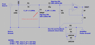
"Another thing is that the LTP input needs a RF shunt as high source impedances directly alter the LTP Gm and make stability interact with the source impedance. Since this is also a large part of the reason for the phase lead cap, it makes sense to make the input shunt cap >CLG*phaselead. So if your phase lead is 10pF and your amp has a gain of 30, then you want >300pF input shunt capacitance. I like finding little gems of reasoning like this."
@Keantoken:
Isn't the 680pF providing the RF shunt? At High Freq, the 10u is a short so the 680pF will be shunting the input of the amp to ground (i.e. shunting R2). What I could do is move the 680pF to the other side of the 10u cap if you are worried that the ESR/ESL of the 10u will be decoupling the 680pF and amp's input at HF.
Also, can you please explain the logic for the shunt cap being > CLG * phase lead cap value?
I understand the phase lead cap is to shunt the RF resistor to get a zero at High Freq for stability. What I don't follow is how it relates to the RF shunt and the relationship C RF shunt > CLG * phase lead cap came about. (CLG = closed loop gain for those who don't know the acronym)
Attached is the latest schematic of the amp.
Thanks for the input Keantoken,
- Sandro
Attachments
Last edited:
I was meaning more generally in terms of how to think about the value you want for that cap. What if you don't want a LP filter? Well you still need a shunt cap for stability so this gives you an idea what value you might want to pick. The 680p does the job fine.
Most people seem to assume that phase lead is the phase lead cap's only function but it is good to check whether something is doing what you think it is doing. If you do that, especially with slow input transistors you may find the feedback network is not having the expected frequency response. This is because the phase lead cap is not just supplying current for the feedback shunt resistor but also supplying the transistor input capacitance. And the larger input capacitance is the differential capacitance between LTP inputs. Thus since this capacitance and the phase lead cap share current, voltage drop across the diff capacitance will be reflected in the voltage across the phase lead capacitance (or worse, the lack thereof), which manifests as an effective pole or shelf response in the LTP Gm. Thus you often end up needing a phase lead cap NOT because you need extra phase for the VAS or output, but because nothing is charging the LTP diff capacitance and that is causing a pole and associated mayhem.
The same applies to source impedance at the input side. But the phase lead cap is magnified by Miller effect, so to have the equivalent effect on the input side your source capacitance (provided by the input shunt cap) needs to match the effective miller capacitance. Thus multiply the phase lead cap by the closed loop gain and take that as the ballpark value for the input shunt cap.
Note that opamps can use custom input transistors or Darlingtons whereas most amp designs just have a simple LTP with general purpose transistors which will have much much lower input impedance than an opamp input. This is a major factor that leads to many of the differences between discrete amps, power amps, and opamp designs.
Should I work at AD? Do I stand a chance at getting in?
- Home
- Amplifiers
- Solid State
- SW-VFA-01: Audio power amplifier video series