Bottom line: For audio amps you need to degenerate the input stage, this is your best option.
By "Audio amps" here I meant Audio Power Amps. For audio op-amps, you can use undegenerated diff-pairs or multi-tanh.
Hello Sandro ,
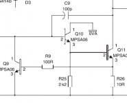
I have a question about your first power amplifier design attached below I have circled the part of the circuit that I have a question about. My question is should'nt the buffered Vas stage you have used need an additional transistor shown in the second image to to protect the Vas. I would of thought apart from the needing a larger transistor there this circuit addition was needed.
The second part of my question is how do you simulate the need to place that transitor there, I have learned through practice that I need this protection transistor but I find it difficult to simulate the failure of this circuit. I hope my question is clear.
Attachments
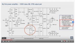
DISCLAIMER: That amplifier was designed when I was in college junior year in 2002 and I knew very little. The point of showing it was not to say it is a great amp (it worked, but had many flaws), but to say I got into designing amps early on.
I built 5 copies of this amp for 5.1 Home theater system, and in most of them, the VAS transistor blew up when I accidentally shorted the output or did something dumb.
1. Output recovery: Drive output of the amplifier to the rail with a square wave. Drive it hard, i.e. if your negative supply voltage is -50V, ask the amp to go to -55V.
Look at the current in the VAS transistor with and without protection transistor (Q9 in your second picture). Does is break the SOA of the transistor?
2. Current limit: Stick a current source in the amplifier output and increase the current into the amplifier. Monitor Q9's and VAS transistor current.
Depending on your current limit topology, the protection transistor may be or may not be part of it. Do the test DC and dynamically using a current square wave.
That is correct. The amplifier shown in that video is the first one I designed when I was in college circa 2002, so it has tons of areas of improvement (third bullet point). The need for the transistor you mention is one of them. Also, the VAS transistor should not be a 2N5551, that was a really poor choice, it is under rated.My question is should'nt the buffered Vas stage you have used need an additional transistor shown in the second image to to protect the Vas.
I built 5 copies of this amp for 5.1 Home theater system, and in most of them, the VAS transistor blew up when I accidentally shorted the output or did something dumb.
Assuming an NPN VAS transistor...The second part of my question is how do you simulate the need to place that transitor there, I have learned through practice that I need this protection transistor but I find it difficult to simulate the failure of this circuit. I hope my question is clear.
1. Output recovery: Drive output of the amplifier to the rail with a square wave. Drive it hard, i.e. if your negative supply voltage is -50V, ask the amp to go to -55V.
Look at the current in the VAS transistor with and without protection transistor (Q9 in your second picture). Does is break the SOA of the transistor?
2. Current limit: Stick a current source in the amplifier output and increase the current into the amplifier. Monitor Q9's and VAS transistor current.
Depending on your current limit topology, the protection transistor may be or may not be part of it. Do the test DC and dynamically using a current square wave.
Hello Sandro,
Sandro I am not being critical of your work , I am testing myself, and am very interested in ways to improve the reliability of amplifiers through simulation before going to a build.
By the way I built an amplifier with exactly the same problem you described in your first build.
Sandro I am not being critical of your work , I am testing myself, and am very interested in ways to improve the reliability of amplifiers through simulation before going to a build.
By the way I built an amplifier with exactly the same problem you described in your first build.
Hi Phoenix, I did not take it as you being critical, just wanted to clarify to anyone looking at that amp what was my goal for showing it in the video.
You are doing the right thing by putting protection and testing before building.
You are doing the right thing by putting protection and testing before building.
Hi all, just to let you know that I just uploaded the next video of the series:
4.2. Audio Amplifier Design Fundamentals: Two Stage voltage feedback amplifier model in LTSpice
4.2. Audio Amplifier Design Fundamentals: Two Stage voltage feedback amplifier model in LTSpice
The video covers the the benefits and best practices for modelling, my library of modelling blocks (attached), and my two stage amplifier model.
Topics in this video:
+ Modelling in LTSPICE
- Why model?
- Sub-circuits you will need
+ Modelling the Two Stage Amplifier VFA
+ LTSpice Demonstration
Next video: How to measure loop gain using LTSpice using dual probes
4.2. Audio Amplifier Design Fundamentals: Two Stage voltage feedback amplifier model in LTSpice
4.2. Audio Amplifier Design Fundamentals: Two Stage voltage feedback amplifier model in LTSpice
The video covers the the benefits and best practices for modelling, my library of modelling blocks (attached), and my two stage amplifier model.
Topics in this video:
+ Modelling in LTSPICE
- Why model?
- Sub-circuits you will need
+ Modelling the Two Stage Amplifier VFA
+ LTSpice Demonstration
Next video: How to measure loop gain using LTSpice using dual probes
Attachments
BTW PHOENIX, I just noticed your name is misspelled. Is it on purpose or is it supposed to be PHEONIX?
Last edited:
Next video
BTW, next video will be on "How to measure loop gain using LTSpice using dual probes". Should have covered this earlier when discussing how to measure loop gain, but I just learnt how to do it in LTSpice (before I did it one at a time).
Acknowledgement to Dave Zan, Tony (ASTX) and Harry Dymond. Learnt the technique while reading their posts in the thread: "2stageEF high performance class AB power amp / 200W8R / 400W4R" by ASTX
Interestingly, I thought I was going to get a million questions about the input stage in the last video ...
Last edited:
Hello Sandro,
I have been holding off.
I like the use of this two transistor arrangement, Walt Jung Jung on DIY has a thread and he attributes the arrangment to Larson (US Patent 3,394,316A). What do you call it.
You have used two very different transistor for the make up of the differential pair stage, the MPSA18 and the KSA992. Why have you done this rather than sticking to the complement of the KSA992.
In real world simulations how close do you get to creating compensation to stop parasitic oscillations from this arrangemen, which I am always concerned with.
Why are you driving this stage with an opamp on both terminals of the diff pair.
I think that the Thompson topology with this treatment of the Cascoded Vas stage would have very low distortion.
Last edited:
Hi Phoenix,
I did not know that Larson came up with the arrangement (luckily his patent is expired). I actually don't have a name for it, should we call it the Larson base current recycler? I have used the arrangement in the past successfully, it works.
Regarding the 2 transistors, given the NPN sees little voltage, wanted to use a high FT, low voltage transistor, hence the MPS18. In this arrangement, the NPN and PNP do not need to be complements. If you have suggestions, for other BJTs that fit the bill let me know. I actually do not know a lot of part numbers, so I have to and search from scratch every time.
If you look at the overall arrangement (op-amp - NPN - PNP), there is a capacitor that by-passes the transistors (C1,C2 in the video schematic). These are your stability caps. Without them, you are playing stability roulette. I actually sized them to 2x what sim said they needed it to be for good stability just in case the op-amp model was wrong. Also the 2x sizing barely changed the distortion. In real word building the arrangement works (with the capacitors). I saw it used in a product from National instruments.
Why the op-amps? For that one you will have to hold off. That will be explained in the future. It does offer quite a few benefits though.
Sorry, but I don't understand what you mean.I think that the Thompson topology with this treatment of the Cascoded Vas stage would have very low distortion.
Hello Sandro,
The compliment of the KSA992 is the KSC1845 . I have read somewhere that you need low impedence to drive the Larson base current recycler for it to work properly.
I will draw up a schematic to show what I mean. Any way look forward to your next video.
The compliment of the KSA992 is the KSC1845 . I have read somewhere that you need low impedence to drive the Larson base current recycler for it to work properly.
I will draw up a schematic to show what I mean. Any way look forward to your next video.
Hi Phoenix, I am curious. If you draw a schematic, I'll take a look.
Thanks for following my video series.
Best, Sandro
Thanks for following my video series.
Best, Sandro
Funny, I've heard the Larsen circuit described as the Boxall current source and the Baxandall current source. Last time I checked, Boxall was the earliest known reference:
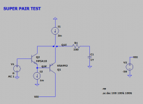
Baxandall Super Pair
The Boxall circuit is problematic if you rely on it's high output impedance to design a circuit and then discover you must reduce it's performance to stabilize it. I've found I never actually needed to use one yet. I played with them a lot in LTspice when I was obsessed with linear sweep generators.
Hi Keane, thanks for the link. Walt Jung is a good dude, he used to work at ADI. I never met him though.
Regarding the circuit, it seems that the common name across all is 'SuperPair', so going forward I'll go with that. What was quite interesting from the thread is that people seem to get some odd behaviors from the circuit. Like oscillations, peaking, etc. I have never seen that.
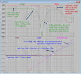
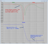
I took my circuit, well a small piece of it, and did some tests. See the attached images. While the curves are wacky, almost all the behaviors are explainable.
The first circuit is a pure trans-conductance cell, with a GM of 1/125. Output variable is IC1. The second circuit is a gain of 10 using using the same trans-conductance cell. Output variable is V(vout). No funny peaking in either.
Sadly, my laptop crashed as I was doing this and lost the test circuit. I would have to draw it again for further testing. Wanted to do some transients, but did not get the chance.
I any case, I'll keep an eye for weird behaviors.
Best, Sandro
Regarding the circuit, it seems that the common name across all is 'SuperPair', so going forward I'll go with that. What was quite interesting from the thread is that people seem to get some odd behaviors from the circuit. Like oscillations, peaking, etc. I have never seen that.
I took my circuit, well a small piece of it, and did some tests. See the attached images. While the curves are wacky, almost all the behaviors are explainable.
The first circuit is a pure trans-conductance cell, with a GM of 1/125. Output variable is IC1. The second circuit is a gain of 10 using using the same trans-conductance cell. Output variable is V(vout). No funny peaking in either.
Sadly, my laptop crashed as I was doing this and lost the test circuit. I would have to draw it again for further testing. Wanted to do some transients, but did not get the chance.
I any case, I'll keep an eye for weird behaviors.
Best, Sandro
Attachments

Hi all, just to let you know that I just uploaded the next video of the series:
4.3. Audio Amplifier Design Fundamentals: Measuring the loop gain of the major and minor loops of an amplifier in LTSpice
4.3. Audio Amplifier Design Fundamentals: Measuring the amplifier major & minor loop gain in LTSpice
The video covers how to measure the loop gain of the major and minor loops in a two stage amplifier. It directly follows from video 4.1.
Topics in this video:
+ The major and minor loops of a two stage amplifier
- The loops in the block diagram
- The loops in the Honey Badger amplifier
+ The Dual Tian simulation method
- Setup
- LTSpice simulation commands
+ LTSpice Demonstration
Materials for the video are attached.
Next video: Introduction to distortion in audio amplifiers
Attachments
Last edited:
Thank you, Sandro you material is so educational and presented so well.
I'm so looking forward to reviewing a few of my designs using your analysis techniques.
Keep up to great work you are really providing and sharing such valuable information to the DIY Audio community.
I'm so looking forward to reviewing a few of my designs using your analysis techniques.
Keep up to great work you are really providing and sharing such valuable information to the DIY Audio community.
Hi all, just a quick ask to everyone watching these videos.
As you know, this is a for fun project for me, and I would deeply appreciate it if you guys subscribed the Youtube channel (Hit the subscribe button).
Also, if you liked the video, to please hit the 'thumbs up button' for the video.
It is not big ask, and takes 2 seconds, and would help me a lot to gauge interest.
Link to channel: SW Audio YouTube Channel
Thanks!
- Sandro
Last edited:

- Home
- Amplifiers
- Solid State
- SW-VFA-01: Audio power amplifier video series