Mr. Jung,
You are one of the leading pioneers of audio and one of the most famous persons in DIY audio world and I doubt if any audio DIYers could have skipped your audio articles and missed your website link.
Anyway, here is my apology again. It was my mistake not being careful enough to read the "restricted" note. I have asked the moderator to delete my posts. I think everything is clear now so let us move on from this.
Regards,
Bill
Last edited:
Mr. Jung,
You are one of the leading pioneers of audio and one of the most famous persons in DIY audio world and I doubt if any audio DIYers could have skipped your audio articles and missed your website link.
Anyway, here is my apology again. It was my mistake not being careful enough to read the "restricted" note. I have asked the moderator to delete my posts. I think everything is clear now so let us move on from this.
Regards,
Bill
Apology accepted here Bill, and my thnx for the kind words. I agree we should move on vis-a-vis the SR.
Let us know how the remote sensing works. There should be no downside to it.
wj
I am planning to stop what I am doing now and restart from scratch because I want to implement a number of changes that I can only do with a new PCB.
In the past couple of days I re-read all of the published articles (form part 1 to 4 as well as the later Improved Positive/Negative Regulators) and got more insight into it. I also studied carefully Jan Didden’s Old Colony PCB design and noted down his thoughts on the current flows of the circuit, etc. I should have done this earlier!
Now I want to design a new PCB with the following changes comparing to my existing PCB:
(1) Have the heatsink electrically floating instead of connecting to GROUND – this is what Jan did in his Old Colony PCB.
(2) Remove the ground plane. Direct ground current with appropriate tracks. I am not sure if I would do a ground shield without covering high current tracks and connected to the quietest point (GND SENSE) like what Jan did in his Old Colony PCB though.
(3) A tighter layout as Jack suggested.
(4) Incorporate protection diodes for the opamps.
(5) Increase the footprints for the onboard 120uF capacitors slightly so that I can mount the Panasonic FR 120uF/50V, the best electrolytic capacitors I can find for the job – low ESL, low ESR and low leakage. This cap is not used for the output. I will look for a higher ESR cap for the output.
(6) Reserve the space for a 5W ceramic wirewound resistor at the output (shunt to ground) to increase the current load of the JSR.
(7) Make two PCBs, one for AD825 SOIC 8 and one for AD817 DIP 8. Compare the sound. I don’t like the idea of using an IC adaptor.
(8) A place holder on the PCB for the 0.01uF capacitor between Sense and GND, so that I can implement the 0.01uF/10R RC for remote sensing, if required. This allows experiment in the future.
(9) Include opamp compensation! discussed below.
I always think that opamp compensation is necessary and here we are using 50MHz devices without compensation! Although people have built numerous JSR successfully without oscillations, I did not have the luck. As my scope photos show, mine had mild oscillations, possibly due to the output and load capacitors having too low ESL/ESR.
Anyway, I like the ideas presented on page 16 in Jung’s article <<Improved Positive/Negative Regulators>>. This session has a title “An Option for Extra Stability and/or RFI Prevention”. It describes the way to insert a 499R resistor at each input of the opamp, a 100pF capacitor to shunt the positive input to ground, and a 100pF to connect the negative input to the output. This is the sort of opamp compensation I see in almost all opamp books.
That would be suitable to replace an existing opamp in a JSR implementation. However, if designing a brand new PCB, I am not sure if that is the best fit.
The reason, I think, is that in the JSR circuit, the positive input is already “low passed” by the 499R/120uF, so the additional 499R/100pF at the positive input is unnecessary. Furthermore, if we introduce the RC for remote sensing, that RC would cover the function of this 499R/120uF. Of course, the 499R/100pF at the positive input will provide more balanced AC input impedance to both the positive and negative inputs of the opamp, but is it necessary?
More below.
Interestingly, in Jung’s latest 2015 <<A Universal Shunt Regulator for Audio Applications>> article, he uses the same sensing circuit as in his JSR but with opamp compensation for his shunt regulator. Here are the differences:
A 499R is inserted into the opamp negative input, and a 33pF connects the negative input to output.
There is no 499R / 33pF at the positive input. But the 499R resistor before the 120uF capacitor has been increased to 1k. This provides better Low Pass function, and provides matching DC impedance to the opamp inputs.
However, the AC impedance is no longer matched between the positive input and negative input.
More below.
So what is the best implementation?
It seems to me that the old JSR circuit has the opamp + / - input impedance matched in both DC and AC. If we introduce opamp compensation, the schema described in <<Improved Positive/Negative Regulators>> will also provide matched opamp + / - input impedance in both DC and AC, but there are more component counts. If we do it in the way as described in <<A Universal Shunt Regulator for Audio Applications>>, then we make the circuit simplified and get better LP function, but we only have DC input impedance matched but not AC for the opamp.
So the question comes down to: Is matching the input impedance in AC important?
I guess for JFET input opamp like AD825, it may not be so important. For bipolar input opamp like AD817, it may be more important.
I am not so sure. I am here to learn. I am yet to decide which way to go. I would like to implement opamp compensation. I can possibly put in place-holders on the PCB so that I can implement them if necessary, or short them out with wires if not necessary. I can also compensate the opamp to different degrees by using different values of capacitors.
Has anyone read this.......https://targetjobs.co.uk/career-sec...h-and-development-rd-industry-sector-overview
Here's a small paragraph,JUST as information.
You will need a technical degree in a discipline related to the field of research in which you want to work – a high level of academic ability is often necessary. For some research positions you may need the extra qualification of a masters or even a doctorate.
Graduates need to have a firm grasp of the basic principles of their discipline as well as to understand the commercial drivers for technology development. Skills in maths, physics and computing will give you an advantage. One of the most important skills you need to demonstrate is an ability to learn and use your initiative. In the early stages of a research project, it’s up to you to understand and define the basic principles of the problem and work out how you might attempt to solve it. In development, engineers need the skills to work in large teams and be able to meet the deadlines of defined schedules.
Here is a question about the JSR.
With the remote sensing 10R 0.01uF RC network as described in the Part 4 document, the AC input amplitude to the error amp has reduced by 10R/1k, or 0.01 or 0.085dB. Does it translate to a 0.085dB reduction in the load regulation of the regulator?
I know 0.085dB is very small considering the extraordinary good performance of the regulator.
Last edited:
Have you tried it in simulation? What did the simulator predict?Does it translate to a 0.085dB reduction in the load regulation of the regulator?
Thanks, Mark.
No, I have not tried it in simulation. I don't have the LTSpice model for the JSR and don't really have the library of components to create one.
I would love if somebody can share the LTSpice model for the JSR.
By the way, I have now redesigned the PCB that has incorporated all items I listed earlier. It now includes opamp compensation for both the + / - inputs, retaining matching impedance for both + /= inputs of the opamp for both AC and DC, same as in Jung's "Improved" document. It also includes a proper implementation of the RC for remote sensing as in the "Part 4" document. I have tightened the PCB tracks as Jack suggested. I am very happy with the result. I have ordered the PCBs from PCBWAY.com and ordered the new parts from Mouser. I expect that I can start building it with the new PCB in about a week's time.
Here is a question about the JSR.
With the remote sensing 10R 0.01uF RC network as described in the Part 4 document, the AC input amplitude to the error amp has reduced by 10R/1k, or 0.01 or 0.085dB. Does it translate to a 0.085dB reduction in the load regulation of the regulator?
I know 0.085dB is very small considering the extraordinary good performance of the regulator.
It translates to a 0.085dB reduction in loop gain of the control loop. It is much, much lower than the variation in loop gain between two opamps of the same type. And much, much lower than loop gain variation with temp. Etc.
No worries!
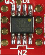
On your plan to lay out two PCBs, one with DIL. other with SMD: with a bit of effort you can have the two footprints together so need only one layout, saving a bit of money. See the diy store PCB.
Jan
Thanks, Jan.
I noticed that AD817 has 8 SOIC as well, so the same footprint will be good for both the AD825 and AD817. So I have abandoned the idea of having 2 PCBs. I will have just one for the 8 SOIC.
No matter how I think of it, I believe that the remote sensing RC should be used and the opamp compensation should be used in all situations. I don't think they have negative impacts on performance. They ensure stability. Once they are in, provided that we don't have stupid amount or stupid value of capacitance at the load to alter the control loop, it will work fine.
Right now I am listening to my system with the active crossover powered by the JSR, the one that showed very mild resonances or probably at the borderline of instability, because I have not replaced the low impedance electrolytic caps at the load. It still sounds a lot better than the standard LM317/337. I am anxiously waiting for the new board and part arrivals.

Rather than remove the posts would it not be better to insert the link in each post? http://www.waltjung.org/PDFs/UnivReg_122714.pdf from References & Regulators | Walt's Blog 2014remove the pictures or delete my entire posts
To do that I think a way is to report your own posts and in the message field ask that the posts are edited with the addition of the links 🙂
I don't think they have negative impacts on performance.
Did that thought emerge fully clothed from the mind of Zeus or do you have some data to validate it?
So, you can try the simple approach, as recommended, without going anywhere. In my mind, it doesn't make any sense whatsoever to actually seek a special high ESR electrolytic. The circuit is stable with Oscons (ultra low ESR) to cheap lytics (high ESR). Lytic values and ESR aren't critical.
But, it appears what you are missing is the differentiation twixt lytics and film/ceramics. There are good reasons why these high-Q types aren't allowed.
I'd suggest that you heed Jan Didden's advice over what LTSpice whispers in your ear. This circuit/topology was developed before LTSpice even existed. That's not to say that LTSpice isn't a great tool (it is), but years of bench experience do count for something, after all.
wj
PS: you know, it would be helpful to those trying help you out to see your actual schematic. You mention the RC net used for remote sensing, but it isn't shown anywhere.
It is actually pretty easy to watch in LTSpice (or any other simulator) the stability impact of a high Q ceramic cap at the output. Below, the loop gain for 100uF (model includes ESR and ESL) and a 100nF ceramic cap with ESR and ESL set to zero. A Tian probe is used for this analysis.
Phase margin is -40 degrees, a clearly unstable loop.
Attachments

Last edited:
Did that thought emerge fully clothed from the mind of Zeus or do you have some data to validate it?
Well, I like the way you do things. But I have neither the equipment nor the knowledge you have to do such tests. Very few people have the equipment you have.
Out of those two choices I made which are in addition to the standard implementation, I have "discovered" the 0.085dB degradation from the RC in remote sensing, which is basically nothing, while theoretically the opamp compensation shouldn't affect anything below 3MHz. We don't want the regulator to regulate beyond 3MHz, do we? I cannot see any reasons that ripple rejections and load regulations to be affected by the opamp compensation below 3MHz.
Last edited:
It is actually pretty easy to watch in LTSpice (or any other simulator) the stability impact of a high Q ceramic cap at the output. Below, the loop gain for 100uF (model includes ESR and ESL) and a 100nF ceramic cap with ESR and ESL set to zero. A Tian probe is used for this analysis.
Phase margin is -40 degrees, a clearly unstable loop.
Thanks. I don't know how to model the "capacitor" out of ground plane / power plane.
When I designed the load board I deliberately designed it so that it has large overlapping areas to minimize inductance, EMI and maximize the "free" capacitance. I measured the capacitance to be as high as 2nF.
So what is the ESL and ESR of this 2nF?
Would you mind replacing your 100nF in your Spice model with 2nF with the same 0 ESR and 0 ESL and let me know the new phase margin?
- Home
- The diyAudio Store
- Super Regulator