Thanks. I don't know how to model the "capacitor" out of ground plane / power plane.
Would you mind replacing your 100nF in your Spice model with 2nF with the same 0 ESR and 0 ESL and let me know the new phase margin?
You ought to learn this stuff, if you ever want to go beyond building kits. Anyway, find below the 2nF case. Not good, ULGF is over 30MHz, meaning the stability will heavily depend on the layout. Very likely it won't be stable in any DIY friendly implementation (through hole parts, generously spaced).
Mr. Jung is entirely correct. No high Q (ceramic) caps at the output of such a regulator. I would suggest even avoiding tantalum or any aluminum polymer devices, just use an old plain electrolytic.
Attachments
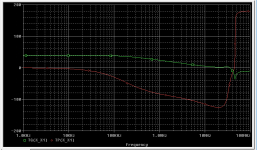
You ought to learn this stuff, if you ever want to go beyond building kits.
When doing HiFi electronics, I wish I were an E.E. I have been a software engineer for most of my life but never studied electronics other than reading a book of <<Electronics for Dummies>> or the sort. I classify myself as a HiFi builder only, not a designer. I love to learn more but life gets so busy with 3 children and a wife and I have to thank heaven that I can spend time building my stuff and talking over here. 🙂
I suspect the power and ground planes at the load may be the prime reason that my JSR had mild resonance, but I don't have evidence. Does it mean I have to redesign the load PCB and get rid of the ground / power planes?
But before that, can anybody explain what ESR and ESL are like with the capacitor formed by the PCB ground and power planes? High or low? I suspect the ESL is low because the distance is short. I don't know for ESR.
Hm, my new PCB will possibly have up to some tens of pF between the power track and the small ground plane on top of it. I have not got rid of the habit of doing it that way trying to minimize track inductance and RFI. The error amp and sensing tracks are not covered by the ground plane to avoid getting noise.
Based on your simulation, some tens of pF should be fine as it will probably affect only the tens of MHz region, and if the opamps are compensated with a -3dB at 3MHz, hopefully, won't cause problems.
What if you add a 499R at the negative input of the opamp, and a 100pF from the negative input to the output?
I have just re-designed my load PCB and removed the power and ground planes and gave the gerber files to the manufacturer. So I will be able to find out if the power and ground planes were the prime reason causing the resonance of the JSR.
I have a few questions.
I'm building a headphone amp which uses 2 PCB's: an output stage with 2SK2013/2SJ313 which pulls 200mA from the +-15V super regulator. And a M2 frontend PCB which has a JFET-buffer of 8 mA.
Do I wire the super regulator first to the output stage, with the sense wires ( which uses the most current) and then to the frontend?
Or just the other way around?
When I wire from the output stage to the front end, I don't use the sense wires anymore?
Or... do I wire in star from the super regulator to the OS PCB and the Frontend PCB and use sense wires both way?
Walter
With Walt's recent work with an LED as a voltage reference in his blog voltage reference GLED 431 would it make sense to replace the LM 329 in the super regulator with 4 LEDS in series. ( Walt shows .55 volt on the current source resistor which leave 1.95 volt as the LEDs voltage so 4 LEDs would be 7.8 volts). it would move the reference voltage point so the v set resistors would have to be scaled accordingly, but it would appear to be a much lower noise reference. Not sure yet if the LEDS would have to be selected for voltage drop at a given current to get some consistency in the new v reference point. And the current feeding the LED reference string adjusted to a value for lowest noise . The LTL4231N LEDs are fairly inexpensive so getting a couple of hundred to select from is cheap. Yes I know it was selected to match the ZTX transistor for voltage consistency in getting a 2.5 volt reference replacing TL431 references. Is lowering the voltage reference noise level worthwhile at this level or is the super regulator's op amp noise level going to dominate and obscure any improvement?
Last edited:
I have a few questions.
I'm building a headphone amp which uses 2 PCB's: an output stage with 2SK2013/2SJ313 which pulls 200mA from the +-15V super regulator. And a M2 frontend PCB which has a JFET-buffer of 8 mA.
Do I wire the super regulator first to the output stage, with the sense wires ( which uses the most current) and then to the frontend?
Or just the other way around?
When I wire from the output stage to the front end, I don't use the sense wires anymore?
Or... do I wire in star from the super regulator to the OS PCB and the Frontend PCB and use sense wires both way?
Walter
Walter, I would wire the sense to the point where the most current variation occurs, which would be the output stage. This is then the point that is best regulated. You can supply the front end from here.
Jan
@ticknpop: The noise in the reference isn't that critical since there is a massive LP-filter. The main noise comes from the opamp only.
Walter, I would wire the sense to the point where the most current variation occurs, which would be the output stage. This is then the point that is best regulated. You can supply the front end from here.
Jan
I think I would attach to the gain stage with the poorest PSRR.
I think I would attach to the gain stage with the poorest PSRR.
Yes, important point. But I am not sure that is best. If you connect the sense to where the most current variation is, you make the supply as flat as possible and that is also good for the point with low PSRR.
The noise getting into the circuit is the product of PSRR and actual supply noise. So decreasing either works. Maybe it is too dependent on the actual implementation to give a general rule.
Jan
From Christer's earlier work on LED noise the voltage across the LED will vary with applied current. So one has to choose the curent that achieves the lowest noise or as Walt likely did choose the current that provides the voltage drop he wanted to match the transistor he choose to make the Gled 431 voltage reference. From Christer's data the LED noise level varies with current, but regardless of the current, the noise is still much lower than standard voltage references noise level.
Last edited:
hi,
I have a question....
Would there be any reason why i couldn't replace the 100-120 uF feedback capacitor with say a 10uF film cap and increase the associated divider resistors accordingly ( around 10 times the original value), assuming it fits the board?
I have a question....
Would there be any reason why i couldn't replace the 100-120 uF feedback capacitor with say a 10uF film cap and increase the associated divider resistors accordingly ( around 10 times the original value), assuming it fits the board?
This cap is hardly necessary since it reduces the gain only 6 dB. It's better though that you keep the low resistance values for the feedback. Just skip those caps if you don't want them.
This cap is hardly necessary since it reduces the gain only 6 dB. It's better though that you keep the low resistance values for the feedback. Just skip those caps if you don't want them.
ok.... thank you.
To clarify the subject, i tried to bypass the electrolytic with small film cap on my 3.3V clock superreg, and although it sounded a bit weird (resonance?), the sound presented signs of lower amount of "noise", which was pleasant.
So i will try without capacitance and with a film cap only, to see what it does.
Is the gain set to 2 or something else?
If you are referring to the voltage divider/feedback part, since i'm using a tl431 for reference (2.5v) at the other op-amp input pin , then the gain is roughly 1.33 i guess (2.5dB)?
I'm using LT6200 op-amp and the build is point-to-point and look stable as is, with a low-pass filter(oscillates without) and without sense wiring.
Now since the film bypass cap seems to lower the noise, than maybe it comes from the resistor and not the electrolytic cap.
I doubt that this 165 MHz could work properly in this design. The opamp has a noise of approx. 1 nV/Hz which means noise near 1 uV with our without this cap. You should not hear any noise.
1 nV/Hz which means noise near 1 uV with our without this cap. You should not hear any noise.
Are you implying that the bypass cap altering the sound is a consequence of op-amp oscillation...?
Maybe it is oscillating, i don't have a scope, but when i tried different feedback flow-pass filters, gradually going to a lower corner frequency, the output voltage lowered a bit as well(oscillation probably)... until i reached around 13 MHz, at which point sharpening the filter didn't do anything. And when i connected, the reg, the voltage was the same.
Anyway, the sound is not irritating for now...i will order some AD817 some time to compare.
Using the super regulator topology with a 741, you can't fail but using a 10 V/us device will became a bit harder and using a 40 MHz device such as AD825 requires some design and pcb layout skills. An AD797 is even harder to get good results with. Using a 165 MHz device such as the LT6200 with point-to-point design and without any calculations, simulations or oscilloscope is more or less impossible to succeed. If the regulator is unstable without using the sense inputs I'll guess you have to redo your homework.
Consider you have a stable function with the opamp itself and have a gain of max 6 dB, that is a achievement but if you insert phase shifting elements such as the the pass transistor D44H11(?) with only 40-50 MHz fT, then you will most likely create stability problems.
Consider you have a stable function with the opamp itself and have a gain of max 6 dB, that is a achievement but if you insert phase shifting elements such as the the pass transistor D44H11(?) with only 40-50 MHz fT, then you will most likely create stability problems.
- Home
- The diyAudio Store
- Super Regulator