sr200 studio refer.
I have make an elektor curve tracer .This is absolutly right method but is more time coast.
regards.
If you have time see here at1.21min http://www.youtube.com/watch?v=M26LSrIB8qAThimios, it is more important to match Ic than Vbe. That is why the voltage across the LTP degeneration should be set to zero, as long as output offset remains a sane value.
I have make an elektor curve tracer .This is absolutly right method but is more time coast.
regards.
Last edited:
All the truth about APEX SR 200 STUDIO REFERANCE
Here.All the truth about Apex SR 200 studio referance - YouTube
Here.All the truth about Apex SR 200 studio referance - YouTube
Thi,
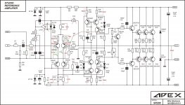
disconnect the DC servo, while you are setting up the correct currents for the amplifier stages.
Set the LTP balance first.
Then check your other currents and the output offset.
Kean agrees with this !!!!
Now back to your comment on matching transistors.
If the hFE is identical at the operational current (900uA) then the base currents will be identical IF and only IF the Ie values are identical.
You must get the Ie values identical and you can check this accurately by measuring across the emitter resistors.
When the Ie are set correctly and the hFE nearly equal you are ensuring base currents are near enough correct, you will be left with an offset in the LTP. This offset is exactly equal to the difference in Vbe of the two LTP transistors when they are passing the correct operational current. This could be 0.1mVbe or 1.2mVbe or 17.6mVbe. That is the error you eliminate or reduce by matching your transistors. You need to match Vbe at the correct operational current. You have 1.1mA and 500uA. You cannot leave this as is.
However, with unmatched transistors that are passing identical Ie, you can vary the source resistance seen by the two bases. Changing the resistance of one, or other, changes the Vdrop to the base and this trims out the residual output offset. BUT you only do this AFTER you have all the other currents set to the correct operational values. When you have all this right then reconnect the DC servo. The servo corrects only the drift in output offset due to temperature changes in the various devices. Since temperature induced drifts are relatively slow, the DC servo is able to keep up and trim the output offset.
sr200 studio refer.
I manage to match transistors with a courve tracer published by elektor.
Hope i do this soon.
Basic is what circuit is functionable so the actions for perfection are recommended
Ιn any case will keep you informed
Again thanks
Best regards.
Thimios.
Dear Adrew thanks for interesting.Thi,
disconnect the DC servo, while you are setting up the correct currents for the amplifier stages.
Set the LTP balance first.
Then check your other currents and the output offset.
Kean agrees with this !!!!
Now back to your comment on matching transistors.
If the hFE is identical at the operational current (900uA) then the base currents will be identical IF and only IF the Ie values are identical.
You must get the Ie values identical and you can check this accurately by measuring across the emitter resistors.
When the Ie are set correctly and the hFE nearly equal you are ensuring base currents are near enough correct, you will be left with an offset in the LTP. This offset is exactly equal to the difference in Vbe of the two LTP transistors when they are passing the correct operational current. This could be 0.1mVbe or 1.2mVbe or 17.6mVbe. That is the error you eliminate or reduce by matching your transistors. You need to match Vbe at the correct operational current. You have 1.1mA and 500uA. You cannot leave this as is.
However, with unmatched transistors that are passing identical Ie, you can vary the source resistance seen by the two bases. Changing the resistance of one, or other, changes the Vdrop to the base and this trims out the residual output offset. BUT you only do this AFTER you have all the other currents set to the correct operational values. When you have all this right then reconnect the DC servo. The servo corrects only the drift in output offset due to temperature changes in the various devices. Since temperature induced drifts are relatively slow, the DC servo is able to keep up and trim the output offset.
I manage to match transistors with a courve tracer published by elektor.
Hope i do this soon.
Basic is what circuit is functionable so the actions for perfection are recommended
Ιn any case will keep you informed
Again thanks
Best regards.
Thimios.
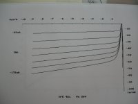
900uA and 25mA per resistor with 8k2 or 500uA and 10mA with 15k value of R11.
This morning i disconnected the servo from sr200 putting out lf411 R5 and R19.
In series with R15 connected two 470uf back to back.
Offset in this case is 100mV.
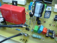
Q1 Q2 is matched pair as you can see on photos.
V on the R12 =24mV
V on the R13=54mV.
Any idea?
Attachments
This morning i disconnected the servo from sr200 putting out lf411 R5 and R19.
In series with R15 connected two 470uf back to back.
Offset in this case is 100mV.
Q1 Q2 is matched pair as you can see on photos.
V on the R12 =24mV
V on the R13=54mV.
Any idea?
Q5 and Q6 must be matched also, offset without servo is about +/-10mV maximum.
Q5 and Q6 must be matched also, offset without servo is about +/-10mV maximum.
Can't remember if Q5 Q6 is matched pair.
I can match this and report again.
Thanks Mr Apex
Kind regards.
sr200 studio refer.
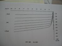
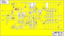
Some measurments on the shematic.
schematic with errors removed
Q5,Q6,Q7,Q8 matched but .....Q5 and Q6 must be matched also, offset without servo is about +/-10mV maximum.
Some measurments on the shematic.
schematic with errors removed
Last edited:
Is a component broken? The two mirrors are way out.
Measure the Vbe of the transistors.
Did you match the equal value resistors?
Measure the Vbe of the transistors.
Did you match the equal value resistors?
sr200 studio refer.
Vbe on Q1=590mV
Vbe on Q2=600mV
ATTENTION post #1268 & #1270 has a tragic mistake not to take into consideration
Sorry for this tragic mistake.Vbe should be 0.8V max
Vbe on Q1=590mV
Vbe on Q2=600mV
ATTENTION post #1268 & #1270 has a tragic mistake not to take into consideration
Attachments
Last edited:
sr200 studio refer.
Any suggestion?
Sorry for this tragic mistake.
Vbe on Q1=590mV
Vbe on Q2=600mV
ATTENTION post #1268 & #1270 has a tragic mistake not to take into consideration
Any suggestion?
query
then the scheme so it would be
Sorry for this tragic mistake.
Vbe on Q1=590mV
Vbe on Q2=600mV
ATTENTION post #1268 & #1270 has a tragic mistake not to take into consideration
then the scheme so it would be
Attachments
sr200 studio refer.
Ιs already at post #1271
then the scheme so it would be
Ιs already at post #1271
exactly.So V12 is 24 mV and V13 is 54mV ?
24mv on R12 =0,5mA
54mV on R13=1.1mA
VR11=(0.5+1.1)*8200=13.1V
Last edited:
Again and again .Something is not working properly.
Have you checked your resistor values?
- Home
- Amplifiers
- Solid State
- Studio Reference Amplifier