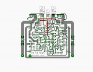
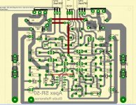
CORRECTION ON SR 50 PCB-my deepest apology...
Correction made:
1. wrong supply of ic (copper wire of pin 7 should be in 4 and vice versa-see pdf)
2. wrong value of r25 should be 100 not 1k
3. wrong value of r26 should be 100 not 1k
4. wrong value of r27 should be 100 not 3k3
5. wrong value of r28 should be 100 not 3k3
Hope this may help(based on the original schematics of SR50).
ENJOY!!!
Correction made:
1. wrong supply of ic (copper wire of pin 7 should be in 4 and vice versa-see pdf)
2. wrong value of r25 should be 100 not 1k
3. wrong value of r26 should be 100 not 1k
4. wrong value of r27 should be 100 not 3k3
5. wrong value of r28 should be 100 not 3k3
Attachments
-
pcb foil pattern with corrected ic supply.pdf38.7 KB · Views: 888
-
schematic of sr 50.pdf23.1 KB · Views: 860
-
top parts placement only names.pdf21.5 KB · Views: 653
-
top parts placement only value.pdf21.8 KB · Views: 649
-
top parts placement with values.pdf23.1 KB · Views: 654
-
top parts with values and copper.pdf50.7 KB · Views: 772
what voltage power supply can i use for 2 pair power output like macd build?and power supply for 1 pair power output?
Hello All!
This is my very first post in this forum🙂
I've been watching for a long time the amplifier topic in this forum, but still haven´t taken my knowledge - my English is also quite bad🙁 Anyway I posted a picture in my amplifier experiments of Apex SR200. It has not been tested yet, heatsink must be machined, as well as the electrolytic caps solder for place, then I will test the amplifier.
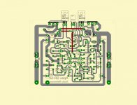
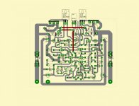
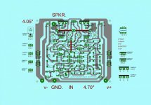
sr-50
SR50 is Studio Ref Amp for small studio monitors without cascode in VAS.
Attachments
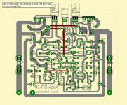
...... you have another smal mistake , se .......😉
ok tell me. I will correct it.🙂
.......and so on ....
..... D1 zenner diode must be reversed , R7=1k resistor in wrog position not to pin 4 IC (not this way )..... , output transistors are the same 2SC5200 ? and so on ........ 🙂
..... D1 zenner diode must be reversed , R7=1k resistor in wrog position not to pin 4 IC (not this way )..... , output transistors are the same 2SC5200 ? and so on ........ 🙂
Last edited:
thanks for the correction
hope this is fine...
..... D1 zenner diode must be reversed , R7=1k resistor in wrog position not to pin 4 IC (not this way )..... , output transistors are the same 2SC5200 ? and so on ........ 🙂
hope this is fine...
Attachments
again, again...
thanks,alex...your the man!
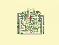
and also change the schematic
....... forget to link , like in pic . 😉
thanks,alex...your the man!
and also change the schematic
Attachments
Last edited:
scematic
thanks,alex...your the man!
and also change the schematic
Attachments
IC1 PIN3 ?
If the unconnected PIN3 floats with PIN2 then the 411 output voltage will always be zerovolts +-output offset +-common mode error.
If the unconnected PIN3 floats with PIN2 then the 411 output voltage will always be zerovolts +-output offset +-common mode error.
Last edited:
you are right
IC1 PIN3 ?
If the unconnected PIN3 floats with PIN2 then the 411 output voltage will always be zerovolts +-output offset.
- Home
- Amplifiers
- Solid State
- Studio Reference Amplifier