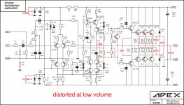
Do you observe the problem in one channel or both chanets?
What are the idle currents of the output transistors and the drivers - in the "bad" channel and the "good" one (if there is a good one)?
What are the idle currents of the output transistors and the drivers - in the "bad" channel and the "good" one (if there is a good one)?
Do you observe the problem in one channel or both chanets?
What are the idle currents of the output transistors and the drivers - in the "bad" channel and the "good" one (if there is a good one)?
thank you for the assist
only right 1 channel not working well, the other channel is good,
and the truth is i do not know how to measure the current on those.
i have tried replacing both driver and pre drivers but still the same problem offset is about 15mV now
thanks
sam
thank you for the assist
only right 1 channel not working well, the other channel is good,
and the truth is i do not know how to measure the current on those.
i have tried replacing both driver and pre drivers but still the same problem offset is about 15mV now
thanks
sam
Hi Sam,
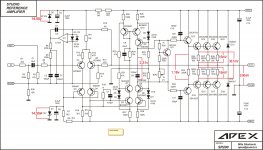
Can you please measure the voltage in both good and bad channels:
1) Across C8;
2) Across R33;
3) Across both R35 and R34 (between the emitters of Q14 and Q15).
Cheers,
Valery
P.S. Referring to the schematic in post #2353
Last edited:
Hi Sam,
Can you please measure the voltage in both good and bad channels:
1) Across C8;
2) Across R33;
3) Across both R35 and R34 (between the emitters of Q14 and Q15).
Cheers,
Valery
got it sir,
ill compare/tell results when i get home from school.
thanks
sam
Hi Tony,
That's what I'm thinking about as well - those measurements are aimed to identify the problematic stage (at least).
Cheers,
Valery
That's what I'm thinking about as well - those measurements are aimed to identify the problematic stage (at least).
Cheers,
Valery
sr200
Good day Sir,
attached are the two measurements
i've check almost all transistor and diodes no problems on components being individually checked.
thanks
sam
Hi Tony,
That's what I'm thinking about as well - those measurements are aimed to identify the problematic stage (at least).
Cheers,
Valery
Good day Sir,
attached are the two measurements
i've check almost all transistor and diodes no problems on components being individually checked.
thanks
sam
Attachments
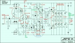
Hi Sam, ok - as I and Tony suspected, OPS in the distorted channel is certainly under-biased. However, OPS itself seems to be fine - the reason is not enough current through the VAS stage. Next step - let's check the voltage drop over R25, R26, R27, R28 in both channels.
Cheers,
Valery
Cheers,
Valery
Good day Sir,
attached are the two measurements
i've check almost all transistor and diodes no problems on components being individually checked.
thanks
sam
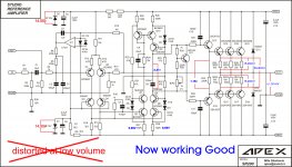
If you look @ named "Good channel" the Bias of output BJTs are
30mV/0R66=45mA/output BJT pair
and the predrivers C4793/A1837 works with 1,16V/220R=5mA
and that`s OK, crossover distorsion are minimized.
With amp witch distort at low volume you have almost "0,0" Bias current,
amp works deep in the class B region
and you can notice high crossover distortion at low levels.
You must increase the bias current with P1 so you can measure with DMM
=30mV across both R35 and R34 (between the emitters of Q14 and Q15).
The amp must run for about 10min to achieve some heatsink temp.
Then readjust bias if necessary.
I will try also increase predriver bias from 5mA to 10mA changing R33 from now 220R to 100R-120R
so also predrivers will have more class A bias current at low and medium volume.
LP
Dragan
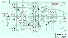
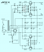
Here are some SR200 voltages and currents thru schematic that`s my help.
Values my vary for some 1-2%
Your -15 volts indication is not correct.
Right, so as soon as Sam shows us his measurements, we will know if we've got that 10mA through the VAS stage emitter resistors (leaving 9mA through the VAS itself).
If that's the case - something's wrong with the bias spreader.
If not - we move our checks further on to the left 😉
If that's the case - something's wrong with the bias spreader.
If not - we move our checks further on to the left 😉
Yupp, my mistake...TXYour -15 volts indication is not correct.
(-)15VDC must be on bases of input diff.cascode.
On picture there is (-)Rail!
Corrected:
Attachments
Last edited:
Hi Sam, ok - as I and Tony suspected, OPS in the distorted channel is certainly under-biased. However, OPS itself seems to be fine - the reason is not enough current through the VAS stage. Next step - let's check the voltage drop over R25, R26, R27, R28 in both channels.
Cheers,
Valery
Here are some SR200 voltages and currents thru schematic that`s my help.
Values my vary for some 1-2%
Good day sir,
i regret that it took a little while before i have replied due to haloween vacation with family.
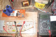
i have found the problem some resistors changed value. i have replace them now working fine. i have attached pics and measurements.
thank you so much for your support, your detailed guide with specific details does not just solved the problem but gave me education how an amp work.
hope to hear more knowledge and skills from you.God bless...
one more thing what do CCS mean?
regards,
sam
Attachments
Hi Sam,
You are welcome, it's good the amplifier works well again
CCS = Constant Current Source
Cheers,
Valery
You are welcome, it's good the amplifier works well again
CCS = Constant Current Source
Cheers,
Valery
Hi Sam,
You are welcome, it's good the amplifier works well again
CCS = Constant Current Source
Cheers,
Valery
i used sr200 amp for programs in our school and planned to try cloning SR800 for my 1900va trafo shown on that picture. since this SR200 seems cannot suffice the 700+ students on open field but must read more.
that is why i asked CCS too.
thanks
regards
i used sr200 amp for programs in our school and planned to try cloning SR800 for my 1900va trafo shown on that picture. since this SR200 seems cannot suffice the 700+ students on open field but must read more.
that is why i asked CCS too.
thanks
regards
"Those on photo" 1K9VA Trafo with 55+55VAC sec will work for max 700-750WRMS@4R0
and with lifted PSU for Input stage and VAS, for about +(7-10)VDC PSU,
...see APEX PSU60 for similarity or my sugestion below,
so the OutputPowerStage (OPS) can work hard klipping till yours trafo sec 55*0,95 VRMS @full power
Those 5% losses (*0,95) are at max loading ratings @4R0 LOAD
And for every 1Arms Output current delivery chose at least +2200uF, for "strong unregulated PSU for OPS"
for example:
800Wrms (we have Vrms and Irms, P is then avarrage, and never is Prms, ...but in DIY we like this way 🙂)
so@4R0
we have: sqrt(800W/4R0)=14,2Arms
so chose Bulk elkos for 14x2200uF=31000uF/rail
Attachments
Last edited:
someone can point me where the BoM is ?
my eyes not good enough to looking at schematic .
thanks
my eyes not good enough to looking at schematic .
thanks
"Those on photo" 1K9VA Trafo with 55+55VAC sec will work for max 700-750WRMS@4R0
and with lifted PSU for Input stage and VAS, for about +(7-10)VDC PSU,
...see APEX PSU60 for similarity or my sugestion below,
so the OutputPowerStage (OPS) can work hard klipping till yours trafo sec 55*0,95 VRMS @full power
Those 5% losses (*0,95) are at max loading ratings @4R0 LOAD
And for every 1Arms Output current delivery chose at least +2200uF, for "strong unregulated PSU for OPS"
for example:
800Wrms (we have Vrms and Irms, P is then avarrage, and never is Prms, ...but in DIY we like this way 🙂)
so@4R0
we have: sqrt(800W/4R0)=14,2Arms
so chose Bulk elkos for 14x2200uF=31000uF/rail
thank you so much for the advice sir, i will then make a list of components for that 800W amp. and try if i can make such amp work.
i will first use that psu 7 for test (shown on pics) using small 42-0-42VAC trafo.
then if succed i will make PCB for PSU75. may i ask which is more reliable 2x15000uf or 3x10000uf per rail? how about caps impedance?
further, does this need to be regulated or not?
thanks,
regards
- Home
- Amplifiers
- Solid State
- Studio Reference Amplifier