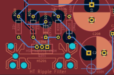
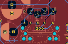
Thank you for the suggestions! I'll solder in a 10k resistor and check. Quite a learning experience, this! Btw. the capacitors C205, C208 and C210 measures good.
We'll get there. It did work! So something changed.
I'd be interested to know voltages/current draw without valves installed on the HT section. Then add in one channel's valves. Then swap channels. You'd expect approx the same channel to channel.
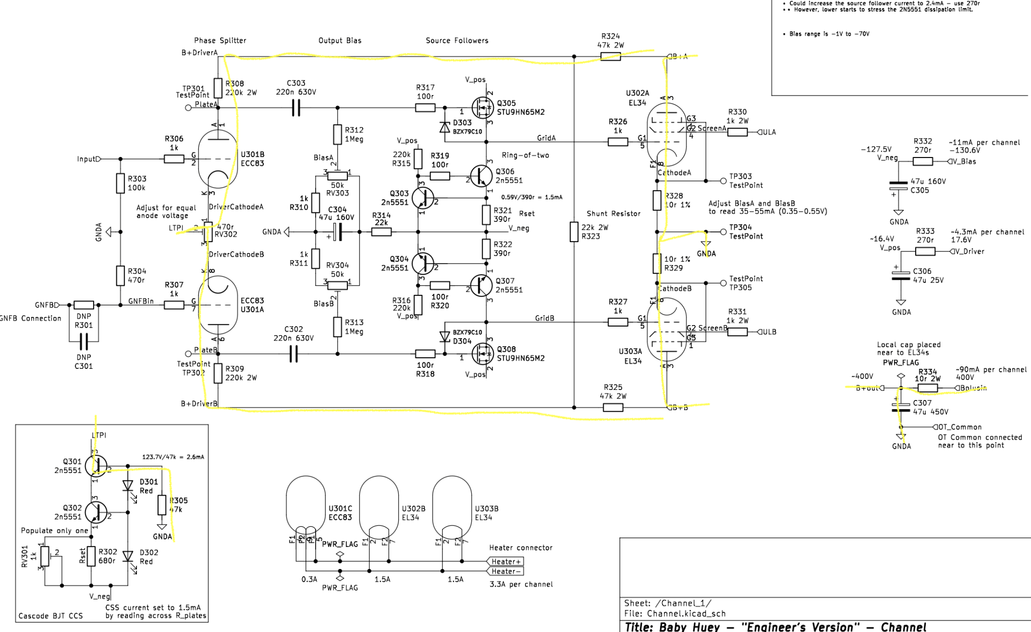
Yellow lines are the current flow on the HT for one channel. So if there's a issue somewhere, it'll be on these runs. With no valves there will be no current, basically, other than any imbalance across R323 and heater elevation. Check across R334 and R434.
Add in the preamp valves - there should be a tiny drop across R334 that your multimeter probably wouldn't measure. Check instead across R305. If OK, add in the EL34s. Check individual currents at TP303 and TP304. Make sure they are sane. Add these together and check across R334.
All I can think is there is a short somewhere that means the FET / diode is burning up. Or perhaps the board is damaged - arcing somewhere? So bypassing the ripple filter section will be telling.
I'd be interested to know voltages/current draw without valves installed on the HT section. Then add in one channel's valves. Then swap channels. You'd expect approx the same channel to channel.
Yellow lines are the current flow on the HT for one channel. So if there's a issue somewhere, it'll be on these runs. With no valves there will be no current, basically, other than any imbalance across R323 and heater elevation. Check across R334 and R434.
Add in the preamp valves - there should be a tiny drop across R334 that your multimeter probably wouldn't measure. Check instead across R305. If OK, add in the EL34s. Check individual currents at TP303 and TP304. Make sure they are sane. Add these together and check across R334.
All I can think is there is a short somewhere that means the FET / diode is burning up. Or perhaps the board is damaged - arcing somewhere? So bypassing the ripple filter section will be telling.
OK! I've done some testing. I first tried to solder in a 10K bypass resistor from C205 to C210, but that resistor started to smoke when I started to turn up the bias. Perhaps you meant a 10R resistor? With no tubes installed, I measured 10V drop across it: 1 mA.
I replaced the 10K resistor with a 10R one, and continued testing with tubes. First each channel individually and then with all tubes installed, and the tubes biased to about 40 mA each.
B+ was 357 V (I think I measured this to about 390 V when I measured it with tubes installed for the first time)
Current trough bypass resistor 160 mA
Current through R334 81 mA
Current through R434 83 mA
Current through both R305 and R405 about 2.4 mA.
All of this seems to add up, more or less?
Sorry - yes, 10r. Should have proofread…
This is encouraging. So all sounds sensible and functioning apart from the capacitor multiplier. With the 10r bridge in place I’d give it a listen. If there’s no audible hum then perhaps you could live without the ripple filter.
If not, all I can think is that the FET you’ve used isn’t suitable for some reason. Perhaps it’s worth a dedicated question in the power supplies area.
Thanks! I'll give it listen. If there is some hum, would it then help with a choke instead of the 10R resistor. I have one at hand from my previous Baby Huey.
I'd go with just the 10R resistor (if you find the hum acceptable). I still don't think we should give up on the capacitor multiplier. If it's not a pain, perhaps take close-up images of both sides of the board in that region. And have a scan about for any charred areas or anything unusual. It's such a simple circuit and layout I can't see how anything could go wrong - unless there's a solder bridge or similar to cause current to flow to the level that would cause the failure...
I've listened to it with the 10R resistor. There is a load hum (load from an audio amplifier) a few seconds after turning the amplifier on, but this gradually lowers to an acceptable level. This level of hum won't be very noticeable from a listening position.
Since I had the amplifier sitting upside down in my Baby Huey maintenance cradle, I put in the choke instead of the 10R resistor just to test. Now there's no hum when turning on and also no hum with my ear close to the speaker.
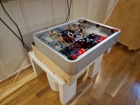
Considering how well the choke works, I might install the choke permanently in the chassis, to keep it as an option if I can't figure out the transistor/diode failure problem.
I'll examine the PCB again very carefully to see if I can see anything amiss.
Since I had the amplifier sitting upside down in my Baby Huey maintenance cradle, I put in the choke instead of the 10R resistor just to test. Now there's no hum when turning on and also no hum with my ear close to the speaker.

Considering how well the choke works, I might install the choke permanently in the chassis, to keep it as an option if I can't figure out the transistor/diode failure problem.
I'll examine the PCB again very carefully to see if I can see anything amiss.
There is a little 100 Hz hum with the choke in place, but it's negligible.
The choke is now mounted in the chassis. There is luckily plenty of space in there. I'll leave it in there for a while. It seems to work quite well.
I couldn't see any signs of anything wrong in the relevant places on the board.
The choke is now mounted in the chassis. There is luckily plenty of space in there. I'll leave it in there for a while. It seems to work quite well.
I couldn't see any signs of anything wrong in the relevant places on the board.
I just took a quick look at alternative FETs. The below looks good:
SIHA22N60AE-GE3
https://www.vishay.com/docs/91924/siha22n60ae.pdf
Also, just checking - you aren't 'over-tightening' the bolt to the heat sink? One of the data sheets lists a maximum torque - made me think...
SIHA22N60AE-GE3
https://www.vishay.com/docs/91924/siha22n60ae.pdf
Also, just checking - you aren't 'over-tightening' the bolt to the heat sink? One of the data sheets lists a maximum torque - made me think...
Thanks! I'll give SIHA22N60AE-GE3 a try.
I don't think I'm over tightening. That would result in some physical damage, like cracks? Haven't had any problems with that before either (I think).
I don't think I'm over tightening. That would result in some physical damage, like cracks? Haven't had any problems with that before either (I think).
That mosfet, like many modern ones, do not show SOA for DC. I usually keep away from those, they can be a bit of a lottery.I just took a quick look at alternative FETs. The below looks good:
SIHA22N60AE-GE3
https://www.vishay.com/docs/91924/siha22n60ae.pdf
Also, just checking - you aren't 'over-tightening' the bolt to the heat sink? One of the data sheets lists a maximum torque - made me think...
Do you know of a suitable mosfet which also is available somewhere reputable?That mosfet, like many modern ones, do not show SOA for DC. I usually keep away from those, they can be a bit of a lottery.
ahh, yeah I see now… So perhaps Pete selected the original with a bit of trial and error. The alternative used here isn’t being used in its SOA, therefore self destructs.That mosfet, like many modern ones, do not show SOA for DC. I usually keep away from those, they can be a bit of a lottery.
Taking that logic, perhaps it would be worth trying one that does have a DC shown on the SOA. Perhaps this:
https://www.mouser.co.uk/datasheet/2/196/Infineon_IPA50R140CP_DS_v02_02_EN-3360271.pdf
This is way above my pay grade. An approach could be to get a few varieties and go through them?
It may be even not enough. I had a similar situation a while ago with a soft start circuit. The mosfet kept blowing away, but the datasheet seemed to say that everything should be OK. The danger here is not only the current and voltage when the power supply it settled, but also the current spike at power up, while C210 is being charged. It means that the voltage across Q201 (referring to the original schematic) is high, and also the current, there is an area where both current and voltage are relatively high, creating a spike of power. It is difficult to simulate the exact conditions, because both the power transformer, the current limiting CL-140 all influence the timings. I would use a mosfet that has a lot of reserve.
Looking in mouser (or digikey/farnell/RS, those are very well respected suppliers):
https://www.mouser.co.uk/datasheet/2/196/Infineon_SPP08N80C3_DS_v02_91_en-1732195.pdf
That one seem to have a wide DC safe area, up to 200mA at ~350V drain-to-source. Should be OK, but with mosfets and high DC voltage, you never know 🙂
PS: I noticed the original schematic uses a 22K resistor for R201, but you use 47K. That increases the HV delay, but also increases the window where the mosfet is "suffering" the increased transient voltage across drain-source.
How about SPP17N80C3? https://no.mouser.com/datasheet/2/196/Infineon_SPP17N80C3_DS_v02_91_en-3363668.pdf
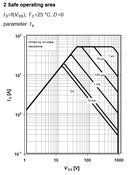
Last edited:
I think you meant SPP17N80C3. Sure, that one should be fine too!How about SPP08N80C3?
Remember isolating washers / thermal transfer pads if you go non-FP packaging. It would open up more possibilities - but potentially also open up thermal issues if the resistance increases between die and heat sink.
[edit - can't read]
[edit - can't read]
Last edited:
Hi, as you are working on this design, I ask you some details I came to over the years.
Do you feel it is needed to have cascoded CCS on phase inverter tail and power drive loads, or simple ones with a zener (to raise the sensing resistor) is enough?
My experience is that it is not needed.
Is it needed to have separate reference voltage for the base of the CCS, or one single is enough as far as negative voltage is low enough not to be overloaded during peaks?
In my experience it is enough to have one reference voltage for all three CCS.
Do you set powerdrive current to fit how many times the minimum requirement for slew-rate?
I use low UL values (around 20%), so input capacitance of the output tubes is low (pentodeish), but still I stay at 5 to 10 times the needed current.
How do you decide the V+ and V- for the powerdrive?
If I stay in AB1 I stay usually at +30 and 3 times the negative biasing voltage. This, together with the above current, usually set the mosfets well below 1 W, so no need to heatsink.
I’ve had an epiphany last week, using higher (43%) UL to triodize the output tubes, then apply positive Shade feedback to have horizontal loadline for the phase splitter, reducing his distortion, then apply an active global negative feedback to recover the damping factor.
Without that global negative feedback I got 0,03% THD at 1 Wrms and 1% THD at 40 Wrms, in both cases is maiy 3rd harmonic, all the others are at least 20 dB below. Applying the active global feedback I should get around 100 times less distortion and a DF around 15.
- Home
- Amplifiers
- Tubes / Valves
- Stereo EL34 Baby Huey Build Log - an "Engineer's Baby Huey"
