Strange , I was using 60V rails - cool. I guess 70+ would do it.
On either EF3 , Driver Re could be increased. I think we were doing 68R = hot ....
OS
On either EF3 , Driver Re could be increased. I think we were doing 68R = hot ....
OS
I did NOT add the 1pF (lead compensation) to the PCB ! I was just playing around with the phase margin in simulation.Looking forward to those IPS boards.
The Wolverine used a high quality ceramic SMD cap (Vishay VJ HIFREQ Series) for the 1pF in the feedback circuit. Any idea if those are good for an even cheaper alternative for the mica caps ?
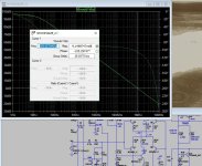
Both the spooky and the Hellraiser use anywhere between 22pF and 47pF as the VAS miller caps. Margin is quite overkill even at 22pF (below)
A ceramic can be used or ...... this - https://www.mouser.com/ProductDetail/Vishay-Vitramon/VJ0603D330JXPAJ?qs=f%2BL2SN1Gfcuaf0MunP%2BrWA==
They can do microwave instrumentation , why not RF ( 1mhz amp).
Hellraiser can not oscillate even without any caps ! Soooo stable. wolverine and Symasui oscillate like hell without a cap.
22pF's on the spook bring unity gain up to 2mhz and reduce 20K THD to 2PPM. 47p = 10PPM. 1-10K THD is flatline 1PPM with
any value .... more OLG <10K.
PS - Wolverine and Symasui are >120db OLG , compensation is "tricky" with them.
OS
Attachments
Last edited:
Oh,i hope that isn't an error 😢I just looked at the Gerbers in the first post. It looks like you have two different board files in the same folder. Each board needs to be in it's own .zip package.
Attachments
Weird, because I'm finding just one set of gerber files both for Spook and Hellraiser...
Gaetano.
Gaetano.
I had to fix those "packages" the spook had some other stuff in there. I hope anybody reviewed those gerbers with a viewer first.
ALL fixed now , even built the output back up from the gerbers.
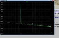
Now , I do the "INFIDEL" .... 25ppb !! - best I've seen.
This might be the "best of the best" (better than wolverine").
Time to move on from Badger's and Wolverines....
Have to drop to 2R load and 120V p-p to even get 1ppm.
OS
ALL fixed now , even built the output back up from the gerbers.
Now , I do the "INFIDEL" .... 25ppb !! - best I've seen.
This might be the "best of the best" (better than wolverine").
Time to move on from Badger's and Wolverines....
Have to drop to 2R load and 120V p-p to even get 1ppm.
OS
Attachments
"I had to fix those "packages" the spook had some other stuff in there. I hope anybody reviewed those gerbers with a viewer first.
ALL fixed now , even built the output back up from the gerbers."
Does it mean that you found errors in gerbers?
ALL fixed now , even built the output back up from the gerbers."
Does it mean that you found errors in gerbers?
No , but there was another amplifier's gerbers in there with it. The full spook was in there without error.
PS - the spook's gerber's were labeled correctly as "SPOOKYAMP_v2.1_IPS_SMD_xxxx .gbr (copper/mask... etc)
Drill data was also - " SPOOKYAMP_v2.1_IPS_SMD.DRL".
PS - the spook's gerber's were labeled correctly as "SPOOKYAMP_v2.1_IPS_SMD_xxxx .gbr (copper/mask... etc)
Drill data was also - " SPOOKYAMP_v2.1_IPS_SMD.DRL".
Last edited:

Spooky PCBs ordered, they should arrive in 3 to 4 weeks. €3.93 for 5 pieces incl. postage and tax. About the price of a glass premium beer on an Amsterdam terras. Will send out the Mouser order when I am holding the PCBs. Curious if I can make them cooperate with the Wolverine (sic) fork of the EF3-3. I 'm confident there will be a way.
Looking at one of your sets of fab files, OST-mini_EF3_gerber I see that
1) You have one hole in which the pad is 3.2mm and the soldermask is 3.8mm. Thus its your 0.6mm offest as they call it?
I am not sure how padstacks are defined in Sprint
2) There is no pad associated with a via, nor a soldermask aperture? So vias get flooded with soldermask, no finish plating either as the via is plugged
3) This ia the file name conventions for JLCPCB, some eCAD tools allow you to pre-define the file extensions
Attachments

Yeah , I did consider whether to make it "ecosystem" friendly. It is -fully , except for the reduced VAS Ic.Wolverine (sic) fork of the EF3-3. I 'm confident there will be a way.
Rsavas , thanks for explaining these points. Which pad is offset .6mm ? All of them ?
OS
I only picked one pad to evaluate, so I assume all of them are the same, assuming that the tool operates in that manner.
By "offset" does that mean the mask is wider than each pad by .6mm. Would it not be better if the mask matched the pad ?
Negative or positive offset .... shifted offset ? Vague ...
OS
Negative or positive offset .... shifted offset ? Vague ...
OS
Yes, assuming that offset is only positive, not sure if sprint will allow a negative offset.By "offset" does that mean the mask is wider than each pad by .6mm.
Usually the SM is set to be slightly larger than the pad, but in certain instances you want it to be the same or less than the pad size. SM defined pads.
This is done to have SM slightly larger so that it can deal with mis-alignment (registration) tolerances to avoid SM on the pad.
That is why specifying the SM in the pad stack allows you to set it as you require for each padstack type. having a global SM offset does not allow this.
Paste mask layer is dealt with similarly to a SM definition, different rules apply and sometimes special shapes are used for a paste process to control the solder paste volume etc.
By default I set SM to be 5mil (0.127mm) over pad and PM to be the same as the pad. On vias. sometimes I make the SM slightly smaller than the pad.
Rick
Last edited:
0.2mm. That's a reasonable number to use. I see it can be applied differently to TH and SM pads, not sure what "other" applies too. Allows for a bit more flexability but not utimately where you define it uniquely to each padstack called out by the part footprint.
Bottomline, good enough for this technology.
Bottomline, good enough for this technology.
Ok, cool. I changed to .2mm for through-hole stuff. I used the default (.1mm) for my current posted SMD work.
OS
OS
Oh , any other suggestions on any of these boards ? I considered "creep" , what signals are going on what trace , and overall
visual impact of the final output.
I also fed back what the real world results were from the (wolverine team). One member there submitted a real nice protection
scheme and even used the "protect" jack on the wolverine boards - I kept that.
I put the fuses on my power board , but I was thinking of a "MOSFET crowbar" scheme that would fully disconnect the power rails
at fault. Any other ideas.
I want to end up with at least 6 different topologies to offer with the 3 power/OPS boards.
Then , address my "weakness" - DOCUMENTATION ! I can't assume everyone just has all this in their heads ??
OS

- Home
- Amplifiers
- Solid State
- Spooky and Hellraiser SMD 60W amps (Wolverine compatible IPS)